

Laser processing method
A laser processing method and pulsed laser technology, which are used in laser welding equipment, metal processing equipment, manufacturing tools, etc., can solve the problems that laser grooves cannot be effectively formed, and the laser beam cannot be set at the bottom of the laser grooves.
- Summary
- Abstract
- Description
- Claims
- Application Information
AI Technical Summary
Problems solved by technology
Method used
Image

Examples
Embodiment Construction
[0027] The laser processing method of the present invention will be described in detail below with reference to the accompanying drawings.
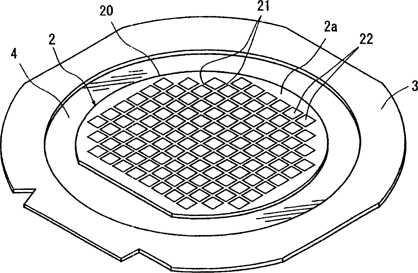
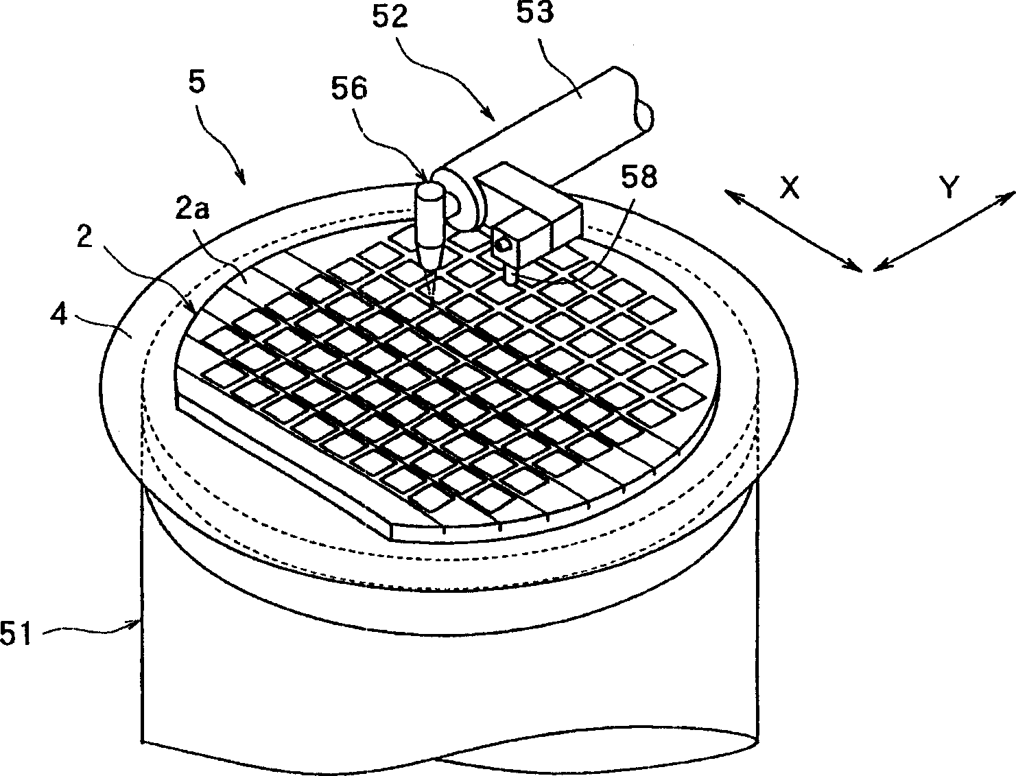
[0028] figure 1 is a perspective view of a semiconductor wafer as a workpiece to be processed by the laser processing method of the present invention. in such as figure 1 In the shown semiconductor wafer 2, a plurality of regions are divided by a plurality of dividing lines 21 provided in a grid pattern on a front surface 20a of a semiconductor substrate 20 such as a GaAs substrate, and in A device 22 such as an IC or LSI is formed in each divided area. The rear surface of the thus constituted semiconductor wafer 2 is placed on the protective tape 4 mounted on the ring frame 3 in such a manner that the front surface 2a, that is, the surface on which the dividing lines 21 and devices 22 are formed, faces upward. .
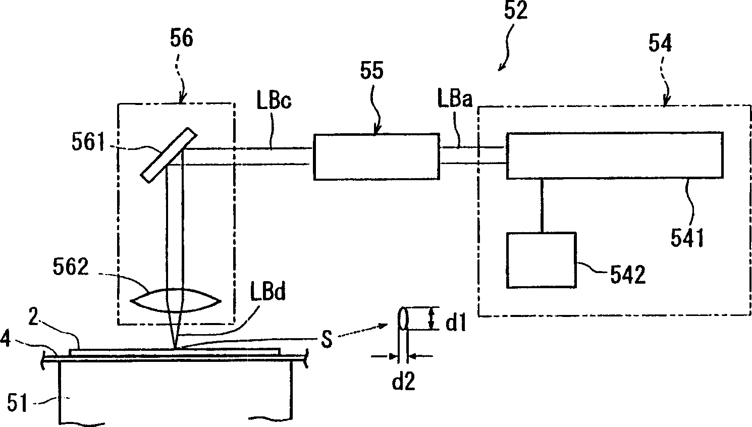
[0029] Figure 2 to Figure 4 A laser beam processing apparatus for carrying out the laser processing method of the prese...
PUM
| Property | Measurement | Unit |
|---|---|---|
| diameter | aaaaa | aaaaa |
| thickness | aaaaa | aaaaa |
| wavelength | aaaaa | aaaaa |
Abstract
Description
Claims
Application Information