Active matrix array device, electronic device having an active matrix array device and picture quality improvement method for such an electronic device

An active matrix and device technology, applied in the field of active matrix array devices, can solve the problems of increasing the cost of active matrix array devices, limited drive signal generation, etc., to achieve the goal of increasing image refresh rate and display area, and improving performance Effect

Inactive Publication Date: 2006-04-05
KONINKLIJKE PHILIPS ELECTRONICS NV
View PDF1 Cites 2 Cited by
  • Summary
  • Abstract
  • Description
  • Claims
  • Application Information

AI Technical Summary

Problems solved by technology

First, it is a complex structure that requires a lot of hardware in the driver circuit, which increases the cost of the active matrix array device
Furthermore, it is limited to ramp voltage based drive signal generation, which means that other driver circuit configurations, like voltage divider type driver circuits that produce a limited number of discrete luminance outputs, cannot benefit from this device

Method used


Image

  • Active matrix array device, electronic device having an active matrix array device and picture quality improvement method for such an electronic device
  • Active matrix array device, electronic device having an active matrix array device and picture quality improvement method for such an electronic device
  • Active matrix array device, electronic device having an active matrix array device and picture quality improvement method for such an electronic device

Examples


Embodiment Construction

[0029] It should be understood that the drawings are merely schematic and not drawn to scale. In particular, some dimensions, such as the thickness of layers or regions, may have been exaggerated while other dimensions have been reduced. It should also be understood that the same reference numerals are used throughout the drawings to indicate the same or similar parts.

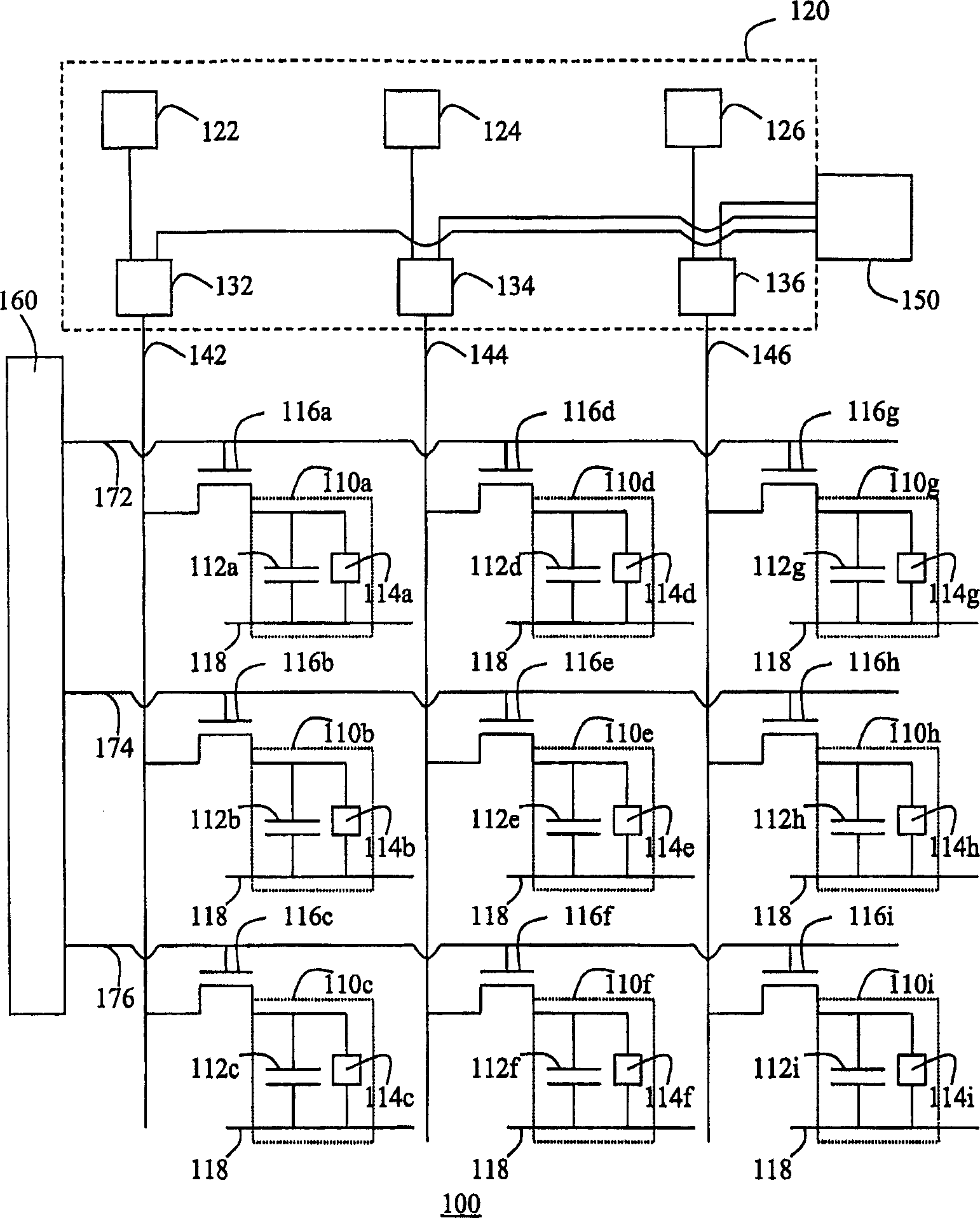
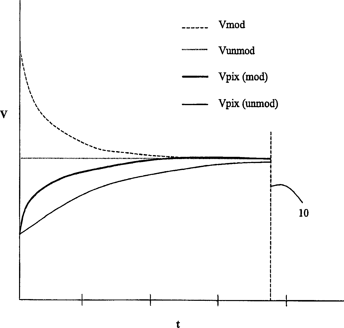
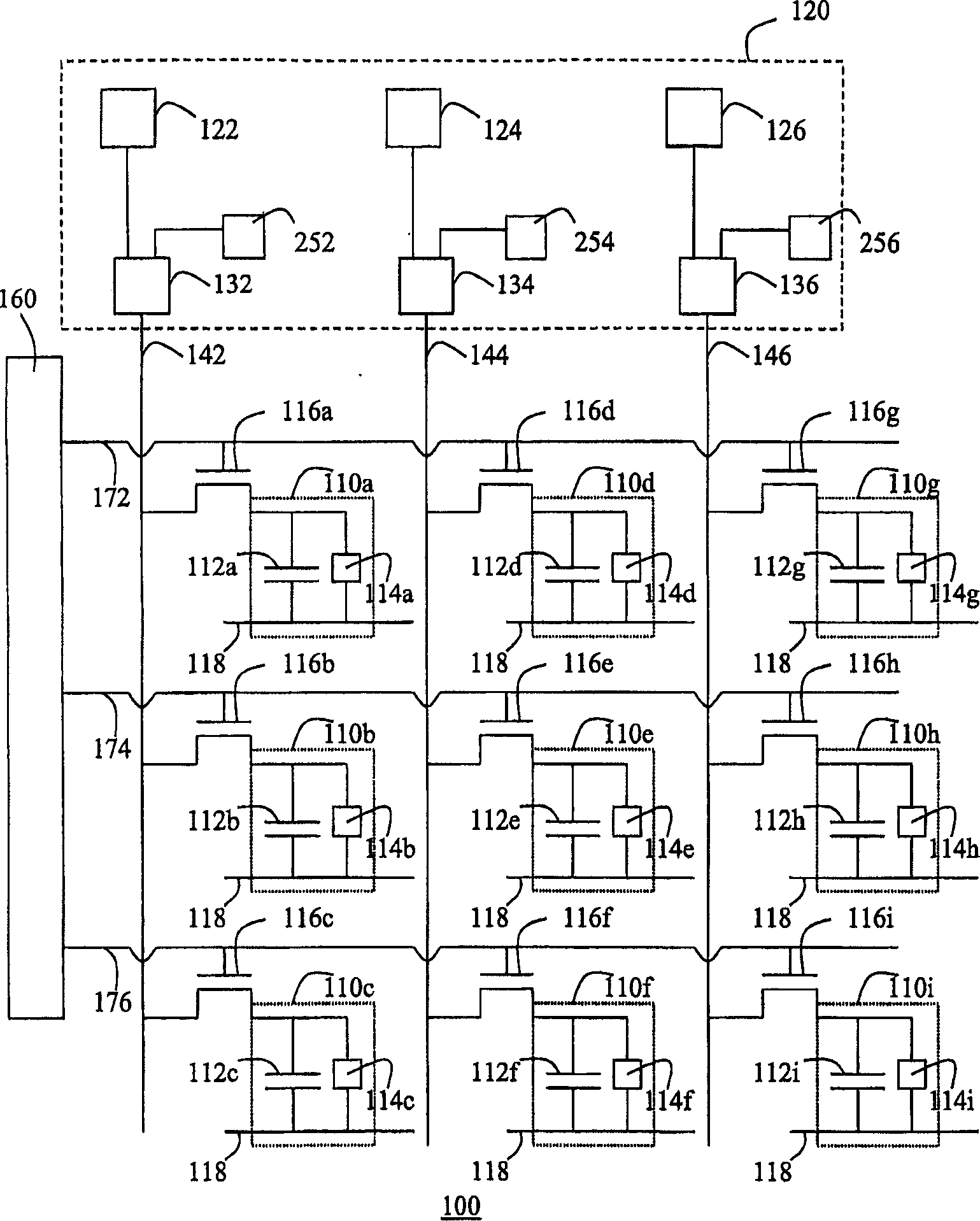
[0030] figure 1 The active matrix array device 100 in has a plurality of active matrix array cells 110a-i, which include corresponding charge storage cells 112a-i and output cells 114a-i, which are also capable of storing a charge. The charge storage units 112a-i are each arranged to maintain the state of one of the output units 114a-i over a predetermined period of time. In case the active matrix array device 100 acts as a display device, the output cells 114a-i may eg be LC or poly-LED cells. exist figure 1 1 , the charge storage units 112 a - i are coupled between respective thin film transistors (TFTs)...


PUM


Abstract

An active matrix array device ( 100 ) has a plurality of active matrix array elements ( 110 a-i), which each have a charge storage element ( 112 a-I) and a capacative output element ( 114 a-I), and which are coupled to respective addressing conductors ( 172, 174, 176 ) and to respective charging conductors ( 142, 144, 146 ) via respective thin film transistors ( 116 a-I). The charging conductors ( 142, 144, 146 ) are coupled to the respective stages ( 122, 124, 126 ) of a driver circuit ( 120 ) via respective voltage modification circuits ( 132, 134, 136 ), which are responsive to respective voltage waveform generators ( 252, 254, 256 ). The respective voltage modification circuits ( 132, 134, 136 ) are arranged to modulate the outputs of the stages ( 122, 124, 126 ) with a voltage waveform from the respective voltage waveform generators ( 252, 254, 256 ) in order to overdrive the addressed matrix array element during a part of its charging cycle. This way, the charge time of the corresponding charge storage element and / or the corresponding output element is reduced.

Description

technical field [0001] The present invention relates to an active matrix array device comprising a plurality of matrix array elements, each matrix array element having a charge storage device. [0002] The invention also relates to an electronic display device having such an active matrix array device. [0003] The invention also relates to a method for improving the image quality of such an electronic display device. Background technique [0004] Active matrix array devices are used in many different fields from sensor-type applications to display-type applications. In the area of ​​larger displays, active matrix array devices are increasingly competing with more traditional cathode ray tube displays as the dominant technology. [0005] In general, a matrix array device has sets of intersections of addressing and charging conductors, with matrix array elements coupled from each set to individual leads at the intersecting intersections. In the case of a matrix array displ...

Claims


Application Information

Patent Timeline
IPC IPC(8): G09G3/36
CPCG09G3/3696G09G2310/0275G09G3/3648G09G3/20G09G3/36G09G3/30
Inventor K·R·惠格特
Owner KONINKLIJKE PHILIPS ELECTRONICS NV
Why Eureka
Try Eureka