Semiconductor device and manufacturing method thereof

A manufacturing method and semiconductor technology, applied in the direction of semiconductor/solid-state device manufacturing, semiconductor devices, semiconductor/solid-state device components, etc., can solve problems such as difficult to form thick films, filling metals, and reduced mechanical strength of semiconductor chips

Inactive Publication Date: 2006-04-12
KK TOSHIBA
View PDF1 Cites 27 Cited by
  • Summary
  • Abstract
  • Description
  • Claims
  • Application Information

AI Technical Summary

Problems solved by technology

[0007] However, the SiO mentioned above 2 layer, Si 3 N 4 It is technically difficult to uniformly form an inorganic insulating layer such as a layer on the inner surface of a through-hole, and in particular, there is a problem that it is difficult to form a thick film.
As mentioned above, the inorganic insulator layer formed by using the existing semiconductor process becomes the main factor that reduces the insulation reliability of the connection plug connecting the front and back sides o

Method used


Image

  • Semiconductor device and manufacturing method thereof
  • Semiconductor device and manufacturing method thereof
  • Semiconductor device and manufacturing method thereof

Examples


Embodiment Construction

[0033] According to the semiconductor device and its manufacturing method according to one aspect of the present invention, it is possible to obtain easily and at low cost the conductor layer insulated by the insulating resin layer with good adhesion to the inner wall surface in the through hole, which is suitable for lamination. A semiconductor device with high insulation reliability, such as a multi-chip package in which multiple semiconductor chips are mounted in layers.

[0034] Hereinafter, the form for carrying out this invention is demonstrated. In addition, in the following description, although embodiment is demonstrated based on drawings, these drawings are provided for illustration only, and this invention is not limited to these drawings.

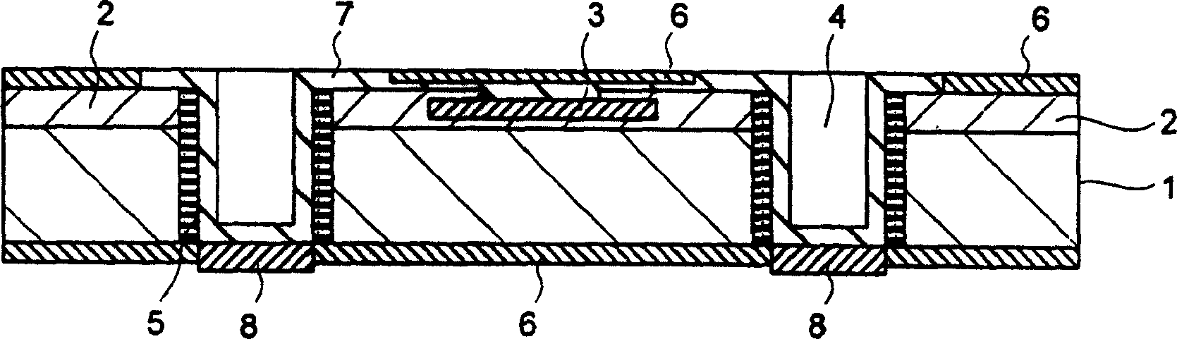
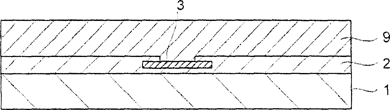
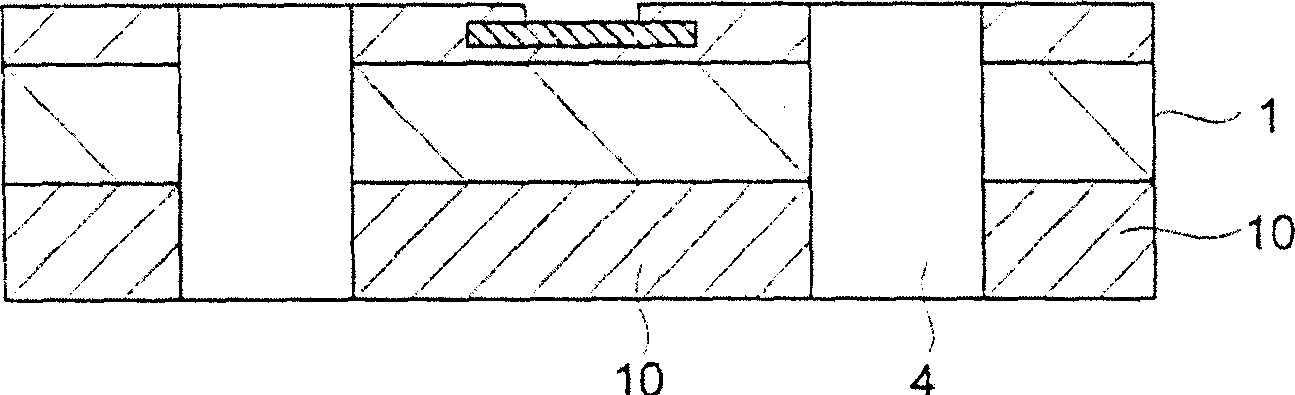
[0035] figure 1 The cross-sectional view of FIG. 1 shows the structure of the semiconductor device according to Embodiment 1 of the present invention. In the figure, reference numeral 1 denotes a semiconductor substrate such a...


PUM


Abstract

A semiconductor device comprises a semiconductor substrate having an through hole, a first insulation resin layer formed on an inner surface of the through hole, a second insulation resin layer formed on at least one of front and rear surfaces of the semiconductor substrate, and a first conductor layer formed in the through hole to connect at least both front and rear surfaces of the semiconductor substrate and insulated from the inner surface of the through hole with the first insulation resin layer. A second conductor layer (wiring pattern) which is electrically connected to the first conductor layer in the through hole is further provided on the second insulation resin layer. The conductor layer formed in the through hole and constituting a connecting plug has a high insulation reliability. Therefore, a semiconductor device suitable for a multi-chip package and the like can be obtained. Further, since the forming ability of the conductor layer connecting the front and rear surfaces and the insulation layer is high, the manufacturing cost can be reduced.

Description

technical field [0001] The present invention relates to a semiconductor device suitable for a multi-chip package on which a plurality of semiconductor elements (semiconductor chips) are mounted, and a method for manufacturing the same. Background technique [0002] In recent years, in order to achieve miniaturization and high-density mounting of semiconductor devices, a stacked multi-chip package in which a plurality of semiconductor elements (chips) are stacked and sealed in one package has been realized. In general, in a stacked multi-chip package, electrical connection between each electrode pad of a plurality of semiconductor chips and an electrode portion of a substrate has been performed by means of wire bonding. In addition, when connecting a plurality of semiconductor chips to each other, electrode pads of the respective semiconductor chips are electrically connected by wire bonding. [0003] Like such a stacked multi-chip package, a package structure in which wire ...

Claims


Application Information

Patent Timeline
IPC IPC(8): H01L23/00H01L23/12H01L23/48H01L25/00H01L25/065H01L21/768H01L21/60H01L21/48
CPCH01L2924/15311H01L2224/16145H01L2224/16225
Inventor 沼田英夫江泽弘和田窪知章高桥健司青木秀夫原田享金子尚史池上浩松尾美惠大村一郎
Owner KK TOSHIBA
Why Eureka
Try Eureka