
Light-emitting component with high lightening effect

A technology with high luminous efficiency and light-emitting elements, which is applied in the direction of electrical components, semiconductor devices, circuits, etc., and can solve the problems of reducing the overall transmittance and limiting the luminous efficiency of light-emitting diodes, etc.

Active Publication Date: 2006-04-12
EPISTAR CORP
View PDF1 Cites 11 Cited by
  • Summary
  • Abstract
  • Description
  • Claims
  • Application Information

AI Technical Summary

Problems solved by technology

However, the thin metal layer will still reduce the overall transmittance, so it will still limit the luminous efficiency of the LED

Method used


Image

  • Light-emitting component with high lightening effect
  • Light-emitting component with high lightening effect
  • Light-emitting component with high lightening effect

Examples


Embodiment Construction

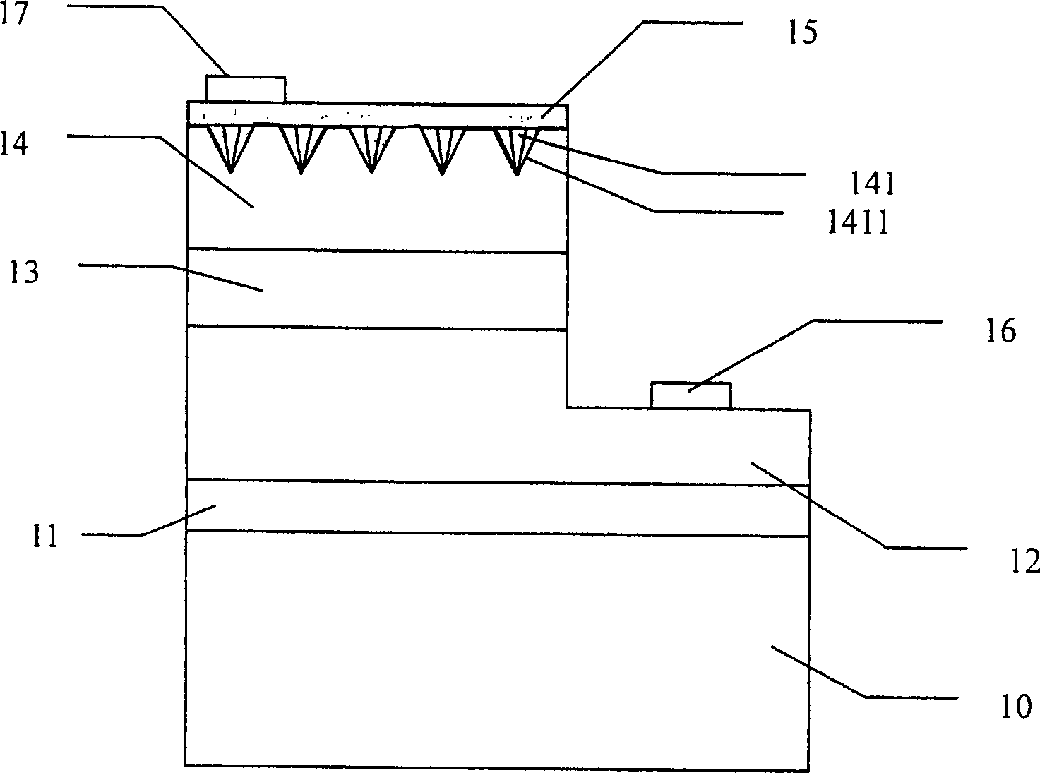
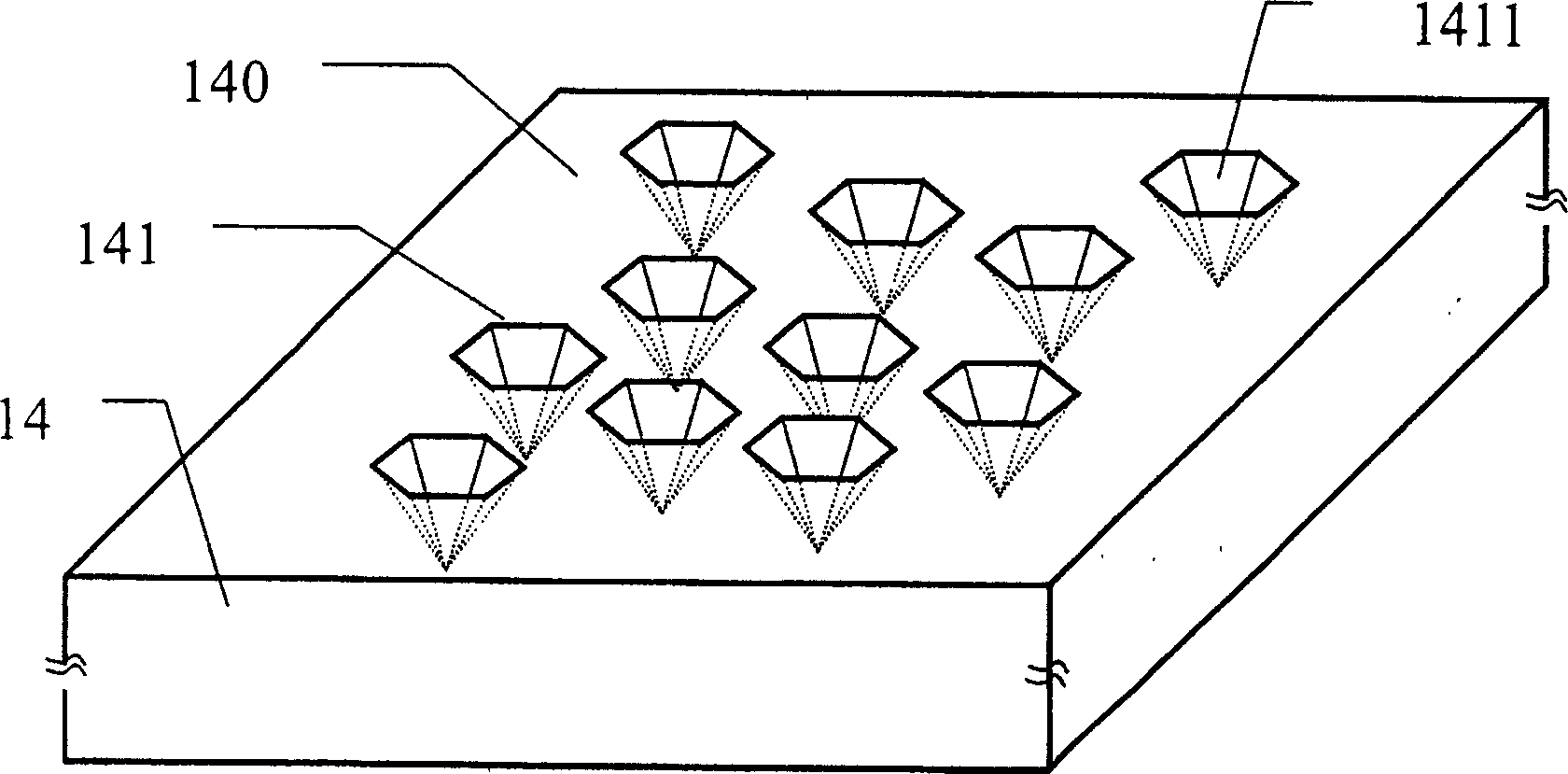
[0037] see figure 1 According to a preferred embodiment of the present invention, a light-emitting element 1 with high luminous efficiency comprises a sapphire substrate 10; a nitride buffer layer 11 formed on the sapphire substrate; a N nitride buffer layer 11 formed on the nitride buffer layer Type nitride semiconductor stack 12, wherein the N-type nitride semiconductor stack 12 includes a first surface and a second surface away from the nitride buffer layer; a nitride multiple quantum well formed on the first surface Light-emitting layer 13; a P-type nitride semiconductor stack 14 formed on the nitride multiple quantum well light-emitting layer, and the surface of the P-type nitride semiconductor stack 14 away from the nitride multiple quantum well light-emitting layer includes a plurality of downward Extended inner hexagonal conical hole structure 141; an oxide transparent conductive layer 15 formed on the P-type nitride semiconductor stack 14 and the inner hexagonal pyram...


PUM

PropertyMeasurementUnit
depthaaaaaaaaaa
depthaaaaaaaaaa
thicknessaaaaaaaaaa

Abstract

A luminous element with high luminous efficiency includes a substrate, a first nitride semiconductor lamina formed on said substrate, a nitride luminous layer formed on it, a second nitride semiconductor lamina formed on the nitride luminous layer, among which, said second nitride semiconductor lamina has multiple downward socket taper holes corresponding to the surface of the nitride luminous layer, an oxide transparent conductive layer formed on the second lamina and the inside surfaces of the socket taper holes of said oxide layer and the second lamina form low resistance ohm contact to reduce the operation voltage of the luminous element and increase the luminous efficiency.

Description

technical field [0001] The invention relates to a light-emitting element, in particular to a light-emitting element with high luminous efficiency. Background technique [0002] Light emitting diodes are widely used, for example, in optical display devices, traffic signs, data storage devices, communication devices, lighting devices, and medical devices. At present, an important subject for technicians is to increase the brightness of light-emitting diodes. [0003] In traditional nitride light-emitting diodes, a thin metal layer (generally Ni / Au series materials) is used as a transparent conductive layer on the surface. However, because most metals have light-shielding properties, the light generated by the light-emitting diode is partly covered by the thin metal layer. Absorption reduces the light transmittance. In order to maintain a certain transmittance, the thickness of the thin metal layer usually needs to be limited to tens to hundreds of angstroms. Nevertheless, th...

Claims


Application Information

Patent Timeline
Patent Type & Authority Applications(China)
IPC IPC(8): H01L33/00H01L33/36H01L33/38
Inventor 欧震林鼎洋赖世国
Owner EPISTAR CORP
Learn More