Liquid crystal panel testing device

A technology for a liquid crystal panel and an inspection device, which can be applied to coupling devices, parts of connecting devices, and test/measurement connectors, etc., can solve problems such as increased manufacturing costs, complicated manufacturing processes, and prolonged manufacturing time.

Inactive Publication Date: 2006-04-26
NHK SPRING CO LTD
View PDF1 Cites 10 Cited by
  • Summary
  • Abstract
  • Description
  • Claims
  • Application Information

AI Technical Summary

Problems solved by technology

[0022] Therefore, the existing inspection equipment for liquid crystal panels cannot mass-produce probe blocks, flexible substrates, and interposer substrates. Since the conductive pattern for terminals of the array glass for liqui...

Method used


Image

  • Liquid crystal panel testing device
  • Liquid crystal panel testing device
  • Liquid crystal panel testing device

Examples


Embodiment Construction

[0041] Embodiments of the present invention will be described in detail below. In addition, the scope of the present invention is not limited to this embodiment.

[0042] The liquid crystal inspection device of the present invention will be described based on the drawings and the following embodiments.

[0043] Embodiments of the present invention will be described below with reference to the drawings. Additionally, with Figure 8 to Figure 13 Partly the same components or components having the same functions are given the same symbols.

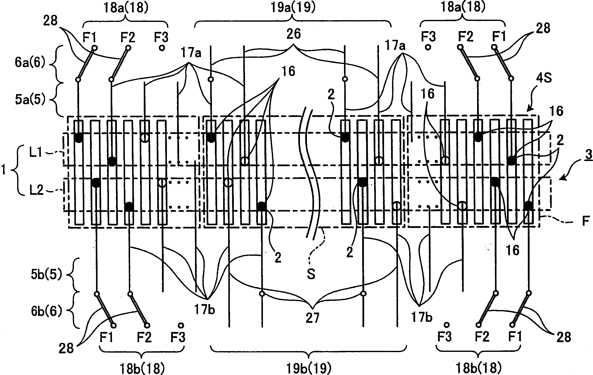
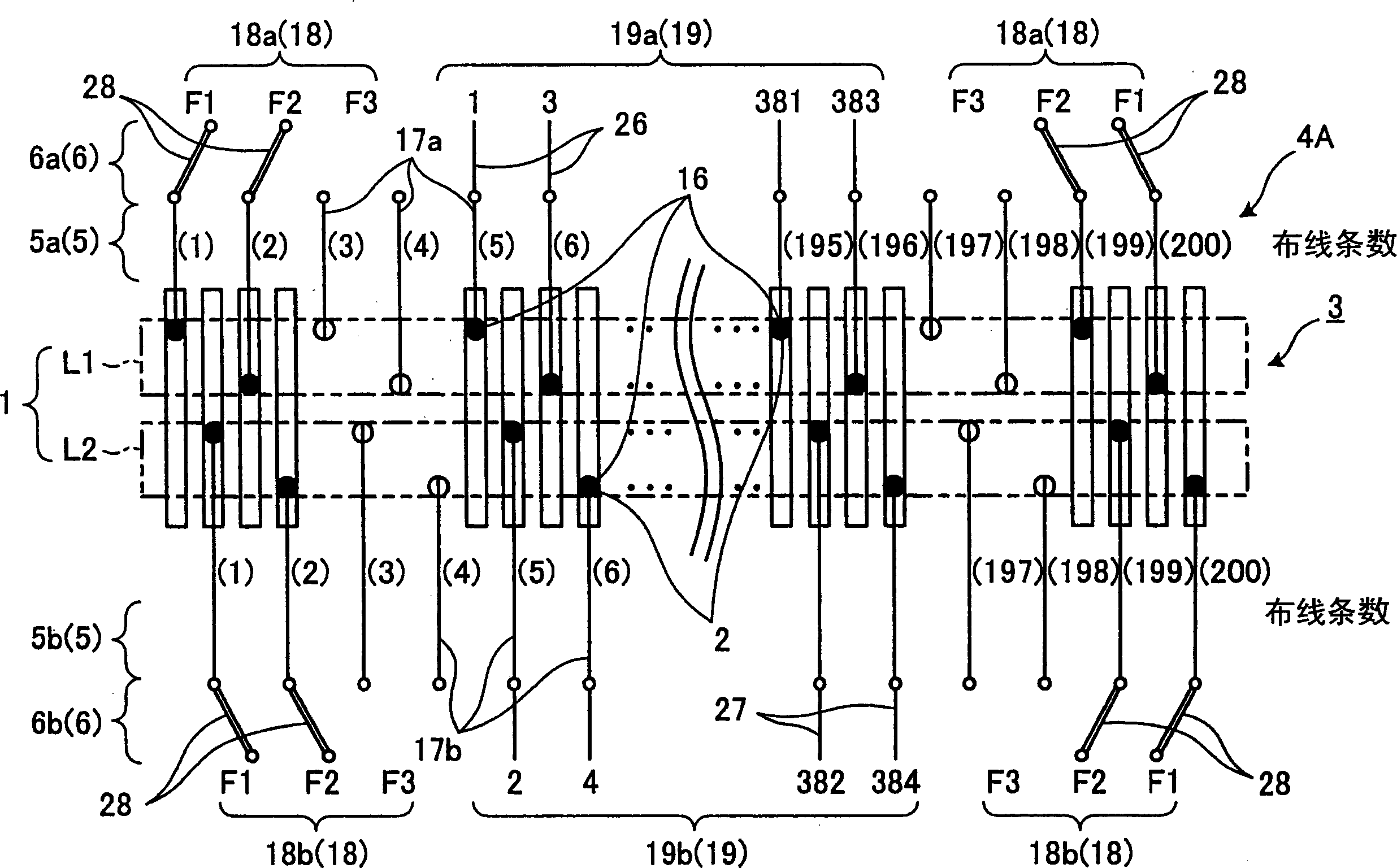
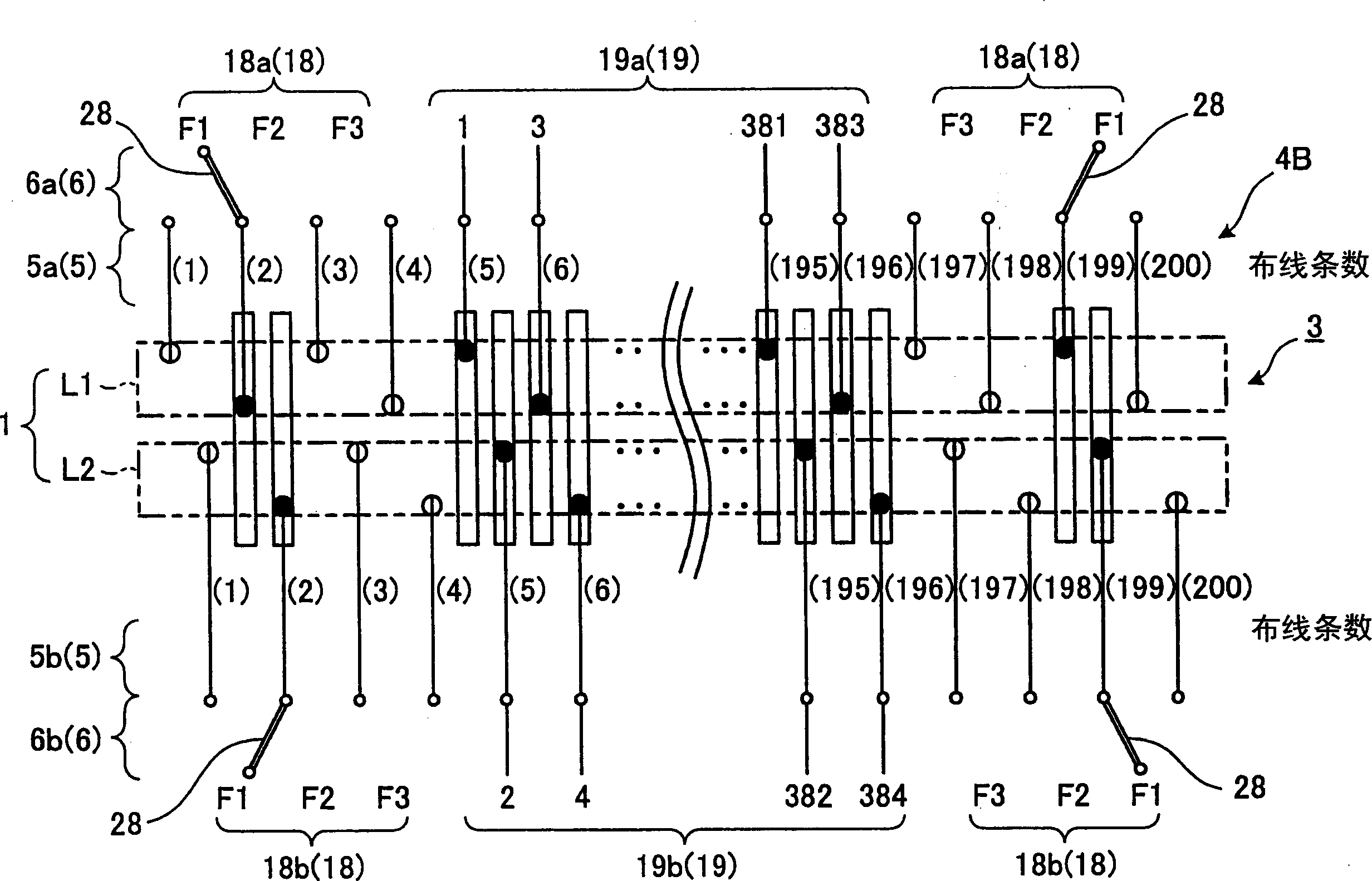
[0044] The liquid crystal panel inspection device of the present invention is configured in the same manner as the conventional device in terms of the overall connection system except for the structure of the components.

[0045] That is, if Figure 8 As shown, the overall connection system applicable to the general liquid crystal panel inspection device of the present invention is structurally such that the probes 2 of the probe block 1 a...


PUM


Abstract

An inspection device for a liquid crystal panel, which is an inspection device for a liquid crystal panel in which a probe (2) of a probe block (1) is brought into contact with a conductive pattern (4) for a terminal of an array glass (3) for a liquid crystal panel for inspection Among them, when the probe block (1) is based on the maximum number of functional lines (F) and signal lines (S) made according to the required specifications of the liquid crystal panel to form the basic terminal conductive pattern (4S), it corresponds to the overall The mode of each wiring forms a plurality of insertion holes (16) for inserting the probes (2), and through inserting the probes (2) in the plurality of insertion holes (16), and forming the array glass ( The terminal of 3) is constituted by the insertion hole (16) in which the wirings of the conductive pattern (4) coincide, while the insertion hole (16) where the probe (2) is not inserted remains empty.

Description

technical field [0001] The present invention relates to an inspection device for a liquid crystal panel that inspects the short-circuit state, open state, TFT characteristics, and pixel characteristics of a conductive pattern printed on an array glass for a liquid crystal panel. Background technique [0002] like Figure 8 As shown, a general inspection device for liquid crystal panels is configured such that the probes 2 of the probe block 1 are brought into contact with the conductive pattern 4 for terminals of the array glass 3 for liquid crystal panels, and the probes 2, one end side The flexible substrate 5 connected to the probe 2 and the relay substrate 6 connected to the other end side of the flexible substrate 5 read the signal from the conductive pattern 4 for the terminal by the detector main body 7. Perform TFT (Thin Film Transistor, Thin Film Transistor) and pixel characteristic inspection. [0003] In this case, the flexible substrate 5 is composed of a flexib...

Claims


Application Information

Patent Timeline
IPC IPC(8): G02F1/1345G02F1/13H01R11/00H01R13/24
CPCH01R13/2421G02F1/1309G02F1/13452G02F2203/69H01R2201/20
Inventor 外间裕康
Owner NHK SPRING CO LTD
Why Eureka
Try Eureka