High transparency touch screen
A touch sensor, transparent conductive layer technology, applied in instruments, coatings, calculations, etc., can solve problems such as changes and changes in electrical signals
- Summary
- Abstract
- Description
- Claims
- Application Information
AI Technical Summary
Problems solved by technology
Method used
Image
Examples
Embodiment Construction
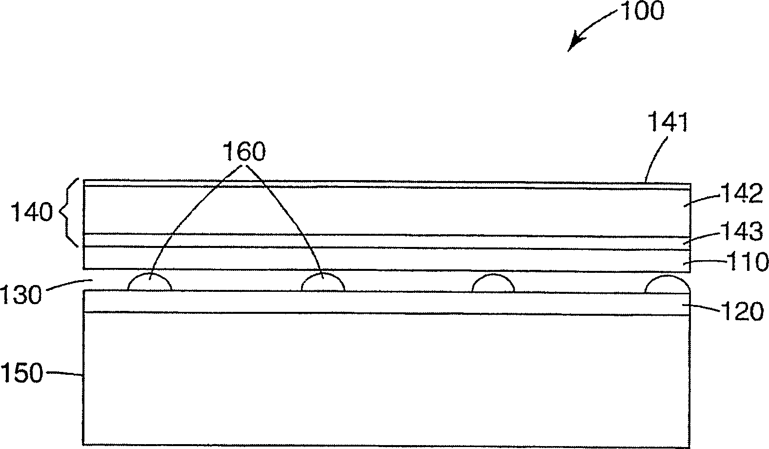
[0015] In the following description of illustrated embodiments, reference is made to the accompanying drawings which form a part hereof, and in which is shown by way of example various embodiments in which the invention may be practiced. It is to be understood that the embodiments may be utilized and structural changes may be made in the embodiments without departing from the scope of the present invention.
[0016] The present invention relates to methods and systems for utilizing transparent conductive elements to enhance light transmission through a touch sensor. For example, resistive and capacitive touch detection methods typically include transparent conductors used as active elements of the touch sensor device. The most widely used transparent conductive oxide for these applications is indium tin oxide (ITO), however other metal oxides such as antimony tin oxide (ATO) and tin oxide (TO), etc. may also be used. Metal / metal oxide stacks can also be used, for example with...
PUM
| Property | Measurement | Unit |
|---|---|---|
| Area | aaaaa | aaaaa |
Abstract
Description
Claims
Application Information
 - R&D
- Intellectual Property
- Life Sciences
- Materials
- Tech Scout
- Unparalleled Data Quality
- Higher Quality Content
- 60% Fewer Hallucinations
Browse by: Latest US Patents, China's latest patents, Technical Efficacy Thesaurus, Application Domain, Technology Topic, Popular Technical Reports.
© 2025 PatSnap. All rights reserved.Legal|Privacy policy|Modern Slavery Act Transparency Statement|Sitemap|About US| Contact US: help@patsnap.com


