A semiconductor structure for electrostatic discharge protection
An electrostatic discharge protection, semiconductor technology, applied in the direction of semiconductor devices, semiconductor/solid-state device manufacturing, semiconductor/solid-state device components, etc.
- Summary
- Abstract
- Description
- Claims
- Application Information
AI Technical Summary
Problems solved by technology
Method used
Image
Examples
Embodiment Construction
[0038] The manner in which preferred embodiments of the invention are made and utilized are discussed in detail below. It should be understood, however, that many of the applicable concepts provided by the present invention can be embodied by various specific words. The specific embodiments discussed herein are merely illustrative of specific ways to make or use the invention, and are not intended to limit the scope of the invention.
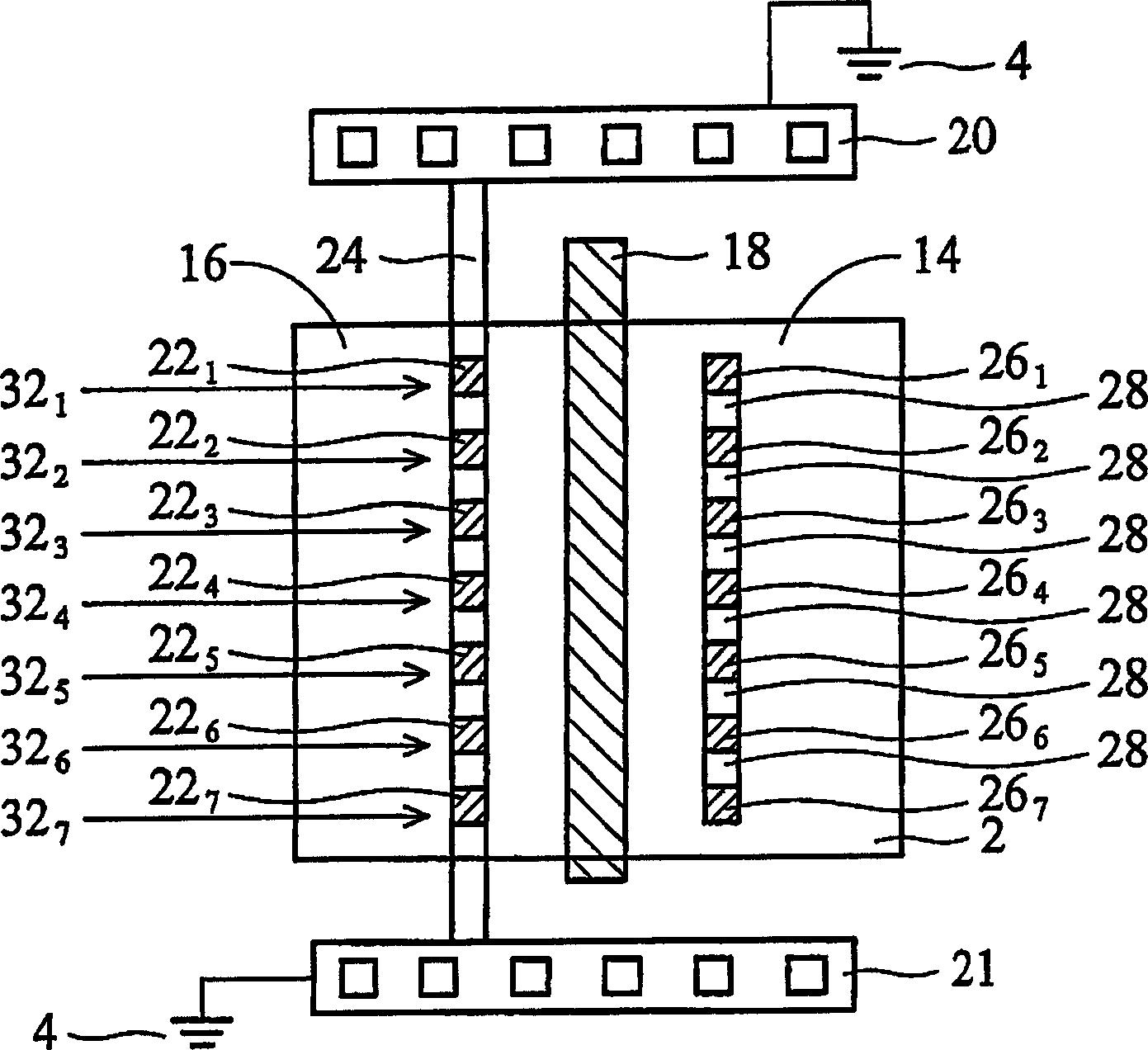
[0039] exist Figure 4 to Figure 9 In the preferred embodiment of the present invention, numerals such as reference numbers are used to designate elements in the embodiments of the present invention for different illustrations and for different descriptive purposes. Figure 4 , Figure 5 as well as Figure 6 It is to present the preferred embodiment from different viewing angles. Figure 4 It is a top view. A gate dielectric is formed on a substrate. A gate 18 is formed over the gate dielectric and preferably has a length of about 0.06 μm ...
PUM
 Abstract
Description
Claims
Application Information


