
Real-time in-line testing of semiconductor wafers

A semiconductor and wafer technology, applied in the field of real-time online testing, which can solve problems such as limited applicability and continuous motion of the substrate

Inactive Publication Date: 2006-05-24
QC SOLUTIONS
View PDF1 Cites 4 Cited by
  • Summary
  • Abstract
  • Description
  • Claims
  • Application Information

AI Technical Summary

Problems solved by technology

During the process, the substrate is not kept in continuous motion, so the applicability of this method for real-time in-line process monitoring is limited

Method used


Image

  • Real-time in-line testing of semiconductor wafers
  • Real-time in-line testing of semiconductor wafers
  • Real-time in-line testing of semiconductor wafers

Examples


Embodiment Construction

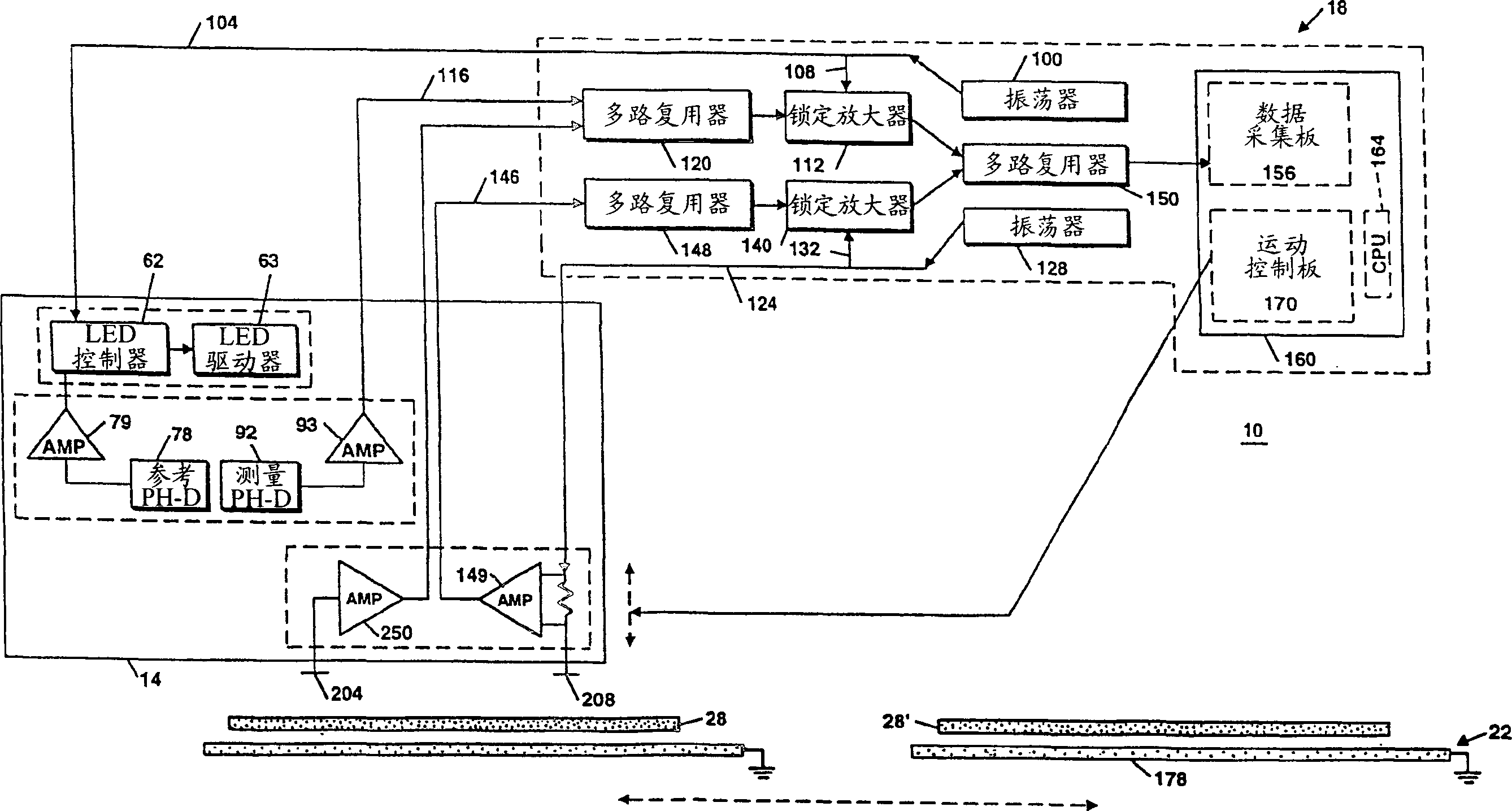
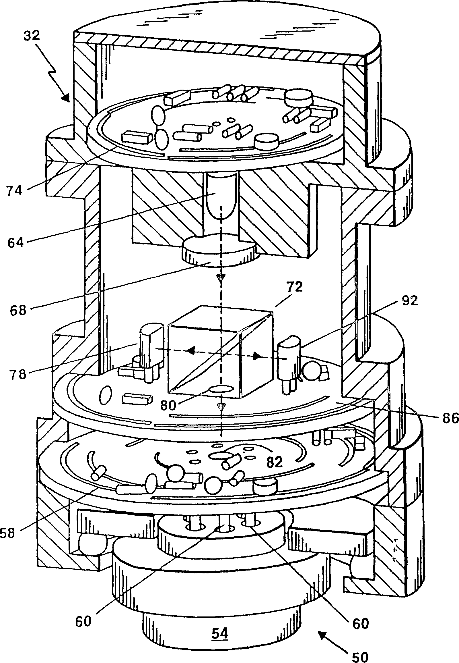
[0020] In one embodiment, the means for performing various electrical characterizations utilize the method disclosed in US Patent No. 4,544,887 for measuring the light-induced voltage at the surface of a semiconductor material, referred to as surface photovoltage (SPV). In this method, a beam of light is directed at a surface region of a sample of semiconductor material, and the light-induced change in electrical potential at the surface is measured. The wavelength of the illuminating beam is selected to be shorter than the wavelength of light corresponding to the energy gap of the semiconductor material under test. The intensity of the light beam is adjusted, the light intensity and the modulation frequency are selected, so that the AC component of the generated induced photovoltage is directly proportional to the light intensity and inversely proportional to the modulation frequency.

[0021] When measurements are made under these conditions, the AC component of the surface ...


PUM


Abstract

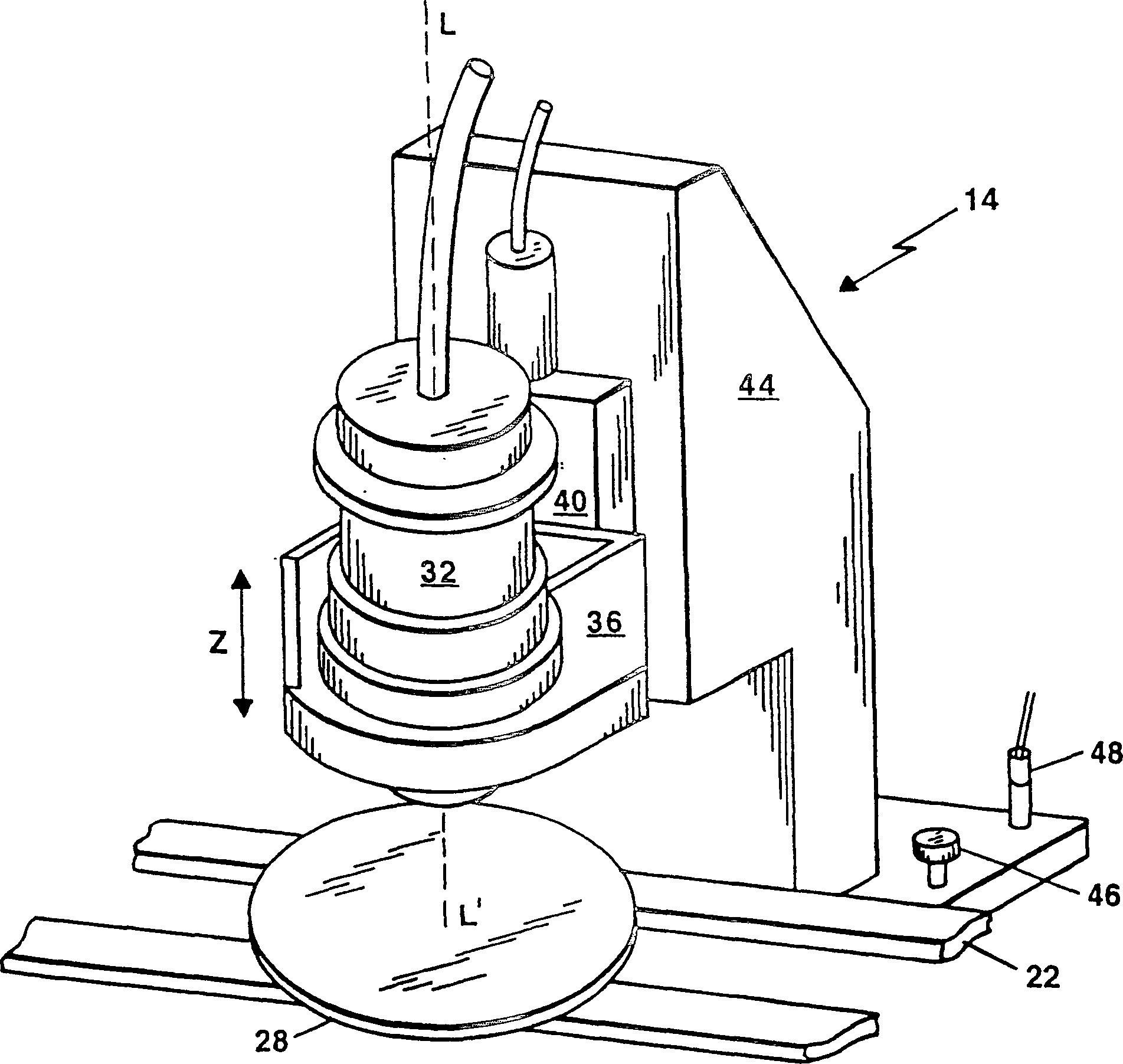
The present invention discloses an apparatus and method for real-time, on-line testing of semiconductor wafers during the manufacturing process. In one embodiment, an apparatus includes a detector assembly within a semiconductor wafer processing line. As each wafer travels into proximity with the detector assembly, a modulated light source within the detector assembly having a predetermined wavelength and modulation frequency illuminates the wafer. Sensors in the detector assembly measure the surface photovoltage induced by the modulated light. A computer then uses the sensed surface photovoltage to determine various electrical properties of the wafer.

Description

technical field [0001] The present invention relates to the testing of semiconductor wafers during manufacture, and more particularly to the real-time in-line testing of semiconductor wafers during the manufacture of integrated circuits. Background technique [0002] In the manufacture of complex integrated circuits (ICs), many individual operations or processing steps are performed in strict sequential order on a silicon wafer. Each of these operations must be precisely controlled to ensure that the overall manufacturing process produces integrated circuits exhibiting the desired electrical characteristics. [0003] Often, failures of individual operations are only detected after the entire very expensive IC manufacturing process has been completed. Due to the extremely high cost of advanced IC manufacturing processes, such failures result in severe financial losses for the integrated circuit manufacturer. Detection of errors immediately after their occurrence during the ...

Claims


Application Information

Patent Timeline
Patent Type & Authority Applications(China)
IPC IPC(8): H01L21/66H01J37/317
CPCH01J37/3171H01J2237/31703H01L22/20H01L2924/0002H01L2924/00
Inventor 爱德华·齐季尔科夫斯基肯尼思·斯蒂普莱斯
Owner QC SOLUTIONS
Learn More