Substrate mounting table, substrate processing apparatus and substrate temperature control method

A temperature control method and substrate processing device technology, applied in the direction of computer control, electrical program control, general control system, etc., can solve the problem of reduced temperature controllability, difficulty in ensuring responsiveness and uniformity of temperature control of the substrate to be processed, difficulty in He gas Uniform diffusion and other issues to achieve good temperature control effect

Inactive Publication Date: 2006-05-31
TOKYO ELECTRON LTD
View PDF2 Cites 23 Cited by
  • Summary
  • Abstract
  • Description
  • Claims
  • Application Information

AI Technical Summary

Problems solved by technology

[0007] However, in the techniques of the above-mentioned Patent Documents 1 and 2, there is a problem that when the height of the protrusion is small, it is difficult to diffuse the He gas for heat conduction uniformly, and it is difficult to ensure the responsiveness and uniformity of the temperature control of the substrate to be processed. If the protrusion is raised to prevent such a problem, the temperature controllability of controlling the temperature of the substrate to be processed in a wide temperature range will be reduced

Method used


Image

  • Substrate mounting table, substrate processing apparatus and substrate temperature control method
  • Substrate mounting table, substrate processing apparatus and substrate temperature control method
  • Substrate mounting table, substrate processing apparatus and substrate temperature control method

Examples


Embodiment Construction

[0071] Next, an embodiment of the present invention will be described with reference to the drawings.

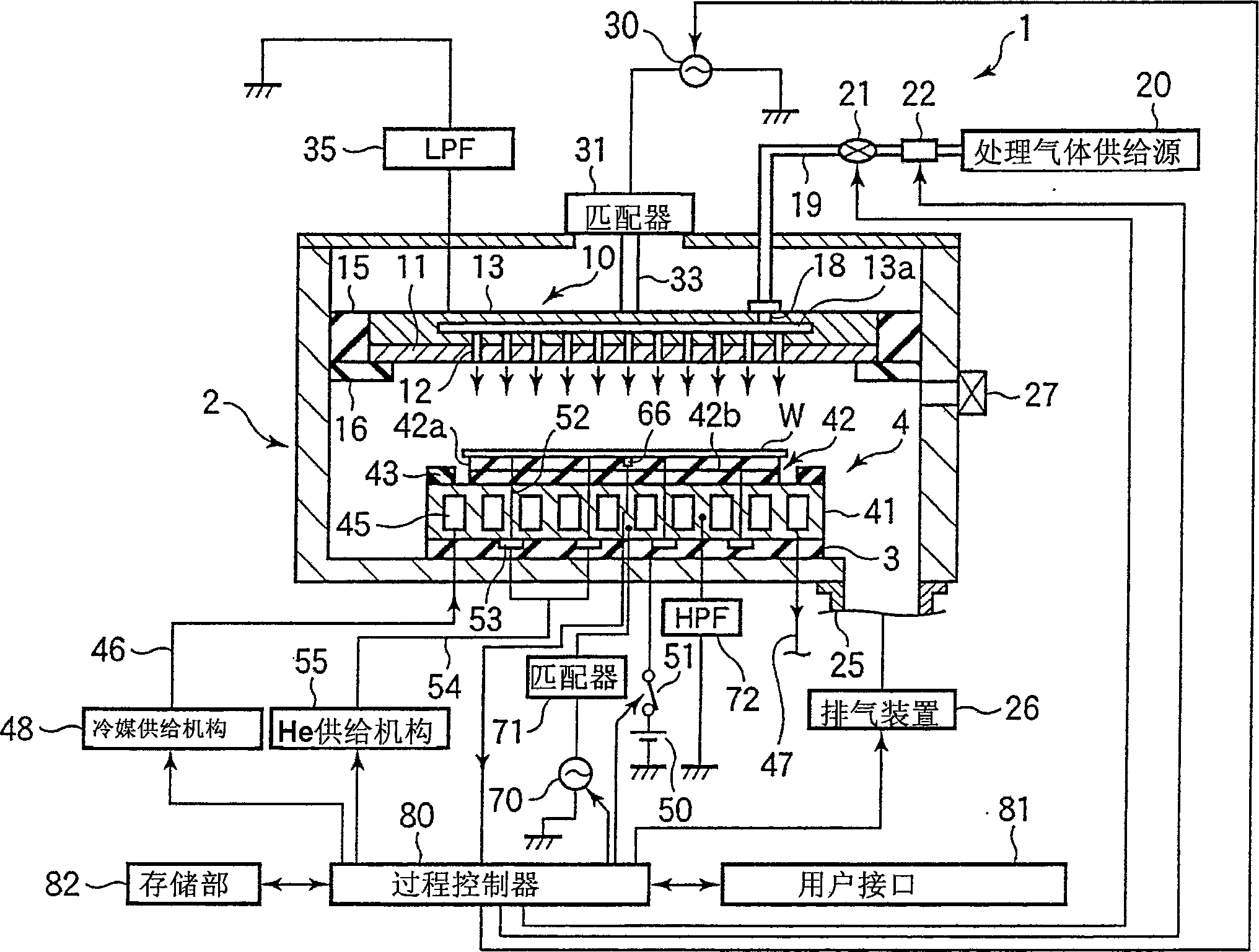
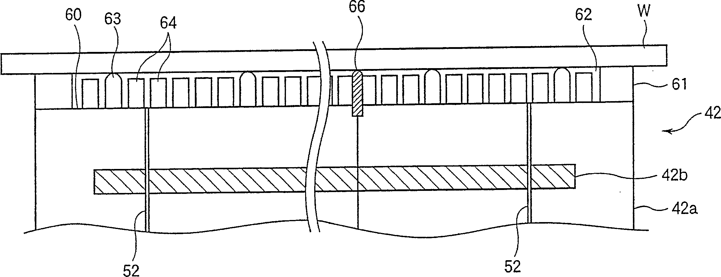
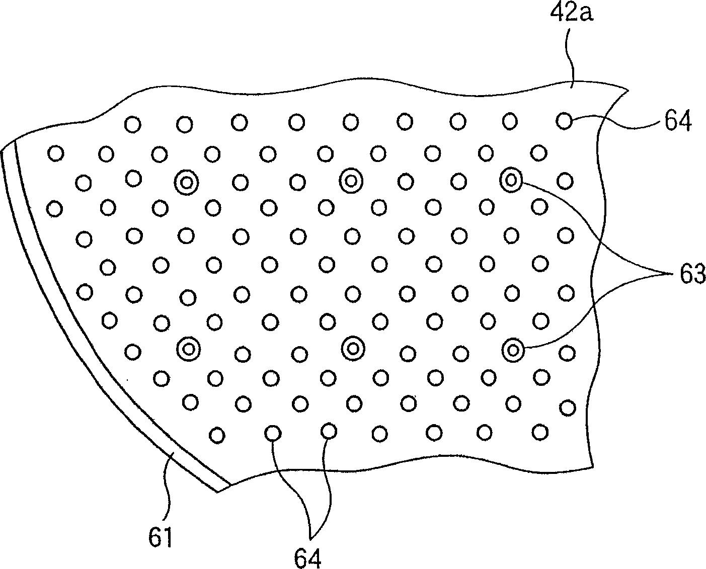
[0072] Here, an example in which the substrate mounting table of the present invention is applied to a plasma processing apparatus will be described. figure 1 It is a cross-sectional view showing a plasma processing apparatus provided with a wafer stage according to an embodiment of the present invention, figure 2 It is an enlarged cross-sectional view showing a main part of a wafer stage according to an embodiment of the present invention.

[0073] The plasma processing apparatus 1 is configured as a parallel plate etching apparatus in which electrode plates face up and down in parallel, and capacitively coupled plasma is formed by a high-frequency electric field formed between them.

[0074] This etching processing apparatus 1 has a chamber 2 which is made of, for example, aluminum whose surface is anodized, and which is formed in a cylindrical shape. At the bottom of t...


PUM


Abstract

The present invention provides a substrate mounting table capable of improving temperature uniformity and temperature control responsiveness of a substrate to be processed and capable of obtaining sufficient temperature controllability. The substrate mounting table (4) used to mount the substrate in the substrate processing device includes: an electrostatic chuck (42), which constitutes the mounting table body; a peripheral ring-shaped protrusion (61), which is formed on the basis of the electrostatic chuck (42). On the surface (60), when the wafer (W) is placed, it is in contact with the peripheral portion of the wafer. At this time, a closed space (62) filled with heat conduction gas is formed at the lower part of the wafer (W); a plurality of first protrusions (63), which is arranged on the inner part of the peripheral annular protrusion (61) of the reference plane (60), contacts with the wafer (W) when the wafer (W) is placed; a plurality of second protrusions (64), set The inner portion of the peripheral annular protrusion (61) on the reference surface (60) is independent from the first protrusion (63), and approaches without contacting the wafer (W) when the wafer (W) is placed.

Description

technical field [0001] The present invention relates to a substrate mounting table for mounting a substrate such as a semiconductor wafer, a substrate processing device for performing dry etching or other processing on a substrate mounted on the substrate mounting table, and a substrate for controlling the temperature of the substrate mounted on the substrate mounting table temperature control method. Background technique [0002] For example, in the manufacturing process of a semiconductor device, plasma processing such as dry etching or sputtering, CVD (Chemical Vapor Growth) or the like is generally performed on a semiconductor wafer as a substrate to be processed. [0003] For example, in a plasma etching process, a mounting table on which a semiconductor wafer (hereinafter simply referred to as wafer) is mounted in a chamber is electrostatically adsorbed and held by an electrostatic chuck constituting the upper portion of the mounting table to form a flow of processing ...

Claims


Application Information

Patent Timeline
Patent Type & Authority Applications(China)
IPC IPC(8): H01L21/683G05B15/00G05B19/04H01L21/00
Inventor 木村英利
Owner TOKYO ELECTRON LTD
Why Eureka
Try Eureka