Optical spot grid array printer

A lithography machine and array technology, which can be used in optomechanical equipment, microlithography exposure equipment, optics, etc., and can solve problems such as unimproved resolution.

Inactive Publication Date: 2006-06-21
APPLIED MATERIALS INC
View PDF2 Cites 23 Cited by
  • Summary
  • Abstract
  • Description
  • Claims
  • Application Information

AI Technical Summary

Problems solved by technology

[0011] Although neither Davidson nor Johnson's systems require a mask, they do not improve the resolution achieved by light-based lithography

Method used


Image

  • Optical spot grid array printer
  • Optical spot grid array printer
  • Optical spot grid array printer

Examples


Embodiment Construction

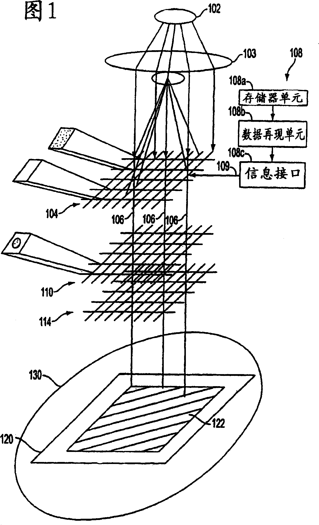
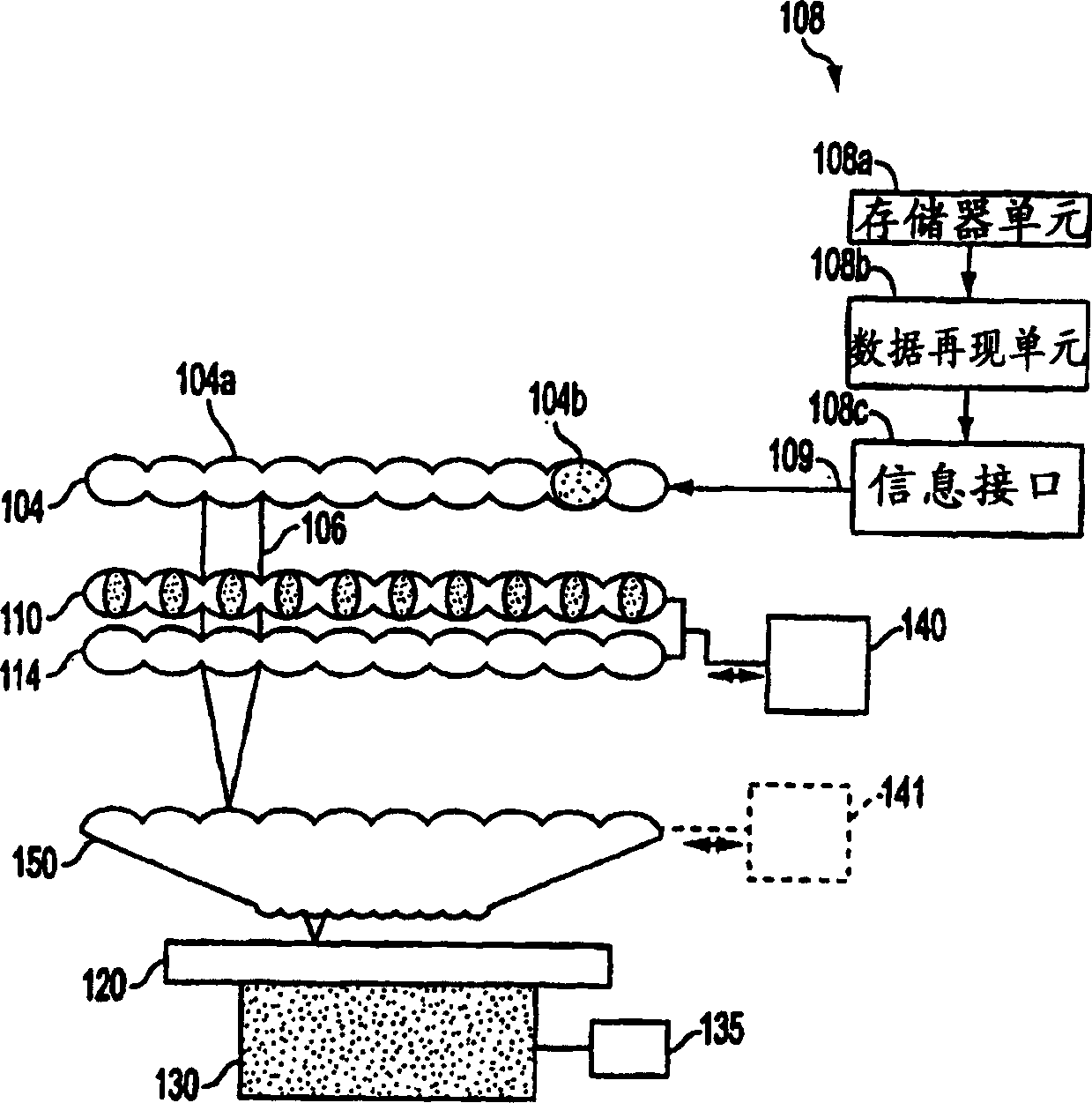
[0032] FIG. 1 shows a photolithography machine according to a first embodiment of the present invention. The lithography machine includes: a light source 102, which may be a continuous wave laser or a pulsed laser; a collimating optical device 103; and a spatial light modulator (SLM) 104, which is used to provide and modulate a two-dimensional array of parallel beams 106 . In response to input data signals 109 provided by programmable image generator 108 , spatial light modulator 104 modulates the beams and controls each beam in synchronization with control stage 130 to expose a desired pattern on substrate 120 . The machine further includes a beam shaper array 110 interposed between the spatial light modulator 104 and the substrate 120 for narrowing each beam 106 to improve resolution. Focusing optics 114 provide a lens element for each beam 106 and focus each beam into small spots on substrate 120 to form a grid array of spaced spots on substrate 102 . The substrate 120 is ...


PUM


Abstract

The present invention provides a high resolution, high data rate dot grid array lithography machine system in which an image is formed by scanning a dot grid array beam over a photoresist coated substrate. High resolution is achieved by apodizing this beam to provide a narrow main lobe. By ensuring that the main lobe does not include energy above the resist threshold, by using memoryless resists and by using sloped, interlaced resists suitable for dot grid array patterning and memoryless properties, it is possible to prevent damage to the substrate. undesired sidelobe recordings.

Description

technical field [0001] The invention relates to a maskless method and device for directly patterning high-definition images on a photoresist layer by using a large array of parallel light beams. The equipment is used in the fabrication of structures for semiconductor devices, microelectronic circuits, microsystems, thin film devices as well as masks and substrates for microlithography applications. [0002] Claiming Priority to a Provisional Patent Application [0003] This patent application claims priority from US Provisional Patent Application Serial No. 60 / 331,029. Background technique [0004] Photolithography is a technique used to transfer images to semiconductor or other substrates. There are two basic types of lithography systems. The first, called image projection lithography, uses a master pattern called a mask or reticle and a projection system to project the image onto the mask or substrate. The second type of system, known as a maskless or direct-write syst...

Claims


Application Information

Patent Timeline
Patent Type & Authority Applications(China)
IPC IPC(8): G03F7/20
CPCG03F7/70275G03F7/70291G03F7/70391G03F7/2057G03F7/7005
Inventor 吉拉德·艾茂基
Owner APPLIED MATERIALS INC
Why Eureka
Try Eureka