
Method for preparing P type ZnO ohmic electrode

A technology of electrodes and electrode materials, which is applied in the manufacture of circuits, electrical components, semiconductors/solid-state devices, etc., can solve problems that affect the performance and stability of devices, it is difficult to explain the ohmic characteristics of electrodes, and poor adhesion of materials, etc., to achieve reduction Poor adhesion, avoiding changes in structure and physical and chemical properties, and protecting electrodes

Inactive Publication Date: 2006-07-12
CHANGCHUN INST OF OPTICS FINE MECHANICS & PHYSICS CHINESE ACAD OF SCI
View PDF0 Cites 2 Cited by
  • Summary
  • Abstract
  • Description
  • Claims
  • Application Information

AI Technical Summary

Benefits of technology

In this new technology called quantum dots (QDS), there're two layers: one made from nickel or gold atoms that help improve its ability to stick onto certain surfaces like silica glasses while maintain their stability during manufacturing processes. Another layer consists mostly of copper oxide nanoparticles - these particles have unique electrical conductivity patterns due to surface plasmon resonance caused by electrons interacted through them. By adding another type of atom called nitrogen gas into both layers, we create strong bonds without causing cracks over long periods of use. Additionally, they enhances the performance of electronic components used near infrared rays, making them more effective against harmful UV radiation than traditional filters designed only towards visible wavelengths. Overall, QDI technologies make better ways to produce nanoelectric elements suitable for various applications including photovoltaics and displays.

Problems solved by technology

The technical problem addressed by this patents relates to improving the efficiency and reliability of manufacturing electronic components with zinc oxide (ZNO) based semi conductors. Previous methods used to make p type gallium nitride films require expensive precious metallization processes or complicated procedures involving multiple steps like ion implantations. There currently no reliable method exists for making highly pure p-Type indium tin oxynitrides without requiring costly rare elements.

Method used


Image

  • Method for preparing P type ZnO ohmic electrode
  • Method for preparing P type ZnO ohmic electrode

Examples


Embodiment 1

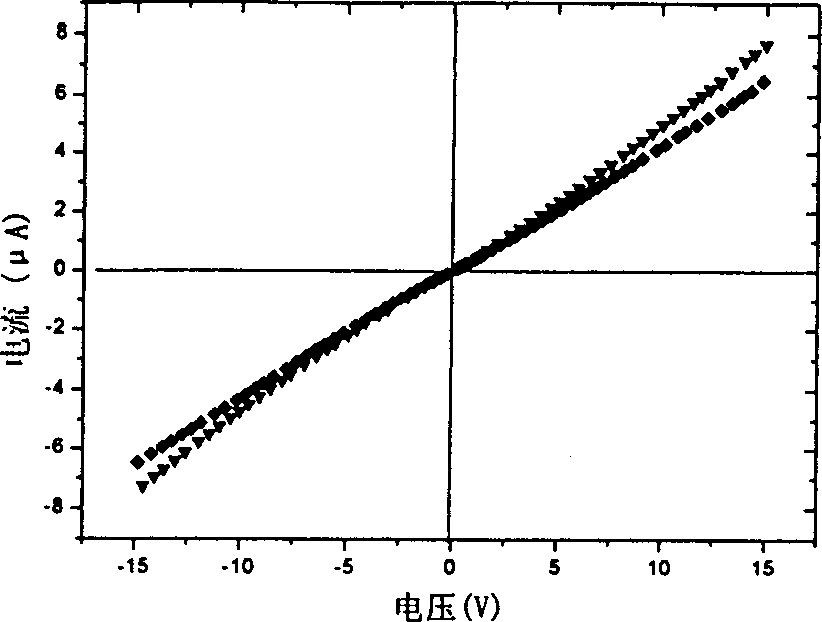
[0014] Example 1, on high-resistance p-type ZnO, after evaporating Ni and Au, rapid thermal annealing is carried out at 200° C. or 300° C. in nitrogen for 150 seconds.

[0015] Selection of experimental conditions:

[0016] The p-type ZnO flakes were grown on sapphire (Al) by molecular beam epitaxy (MBE). 2 o 3 ) on nitrogen-doped high-resistance p-type ZnO with an area of ​​about 1 cm 2 , and its resistivity is about 60Ω·cm.

[0017] Firstly, the p-type ZnO sheet was cleaned by ultrasonic cleaning with acetone and absolute ethanol for 5 minutes; rinsed with deionized water and washed with dry N 2 blow dry. The thickness is 0.2mm and the area is 6×6cm 2 The tantalum sheet is used as a metal mask, and two areas of 1mm are formed on the tantalum sheet by machining. 2 A circular hole is used as the shape of the electrode, the distance between the two electrodes is 2mm, the distance between the mask plate and the evaporation source is 12cm, and the purity of Ni and Au is 99....

Embodiment 2

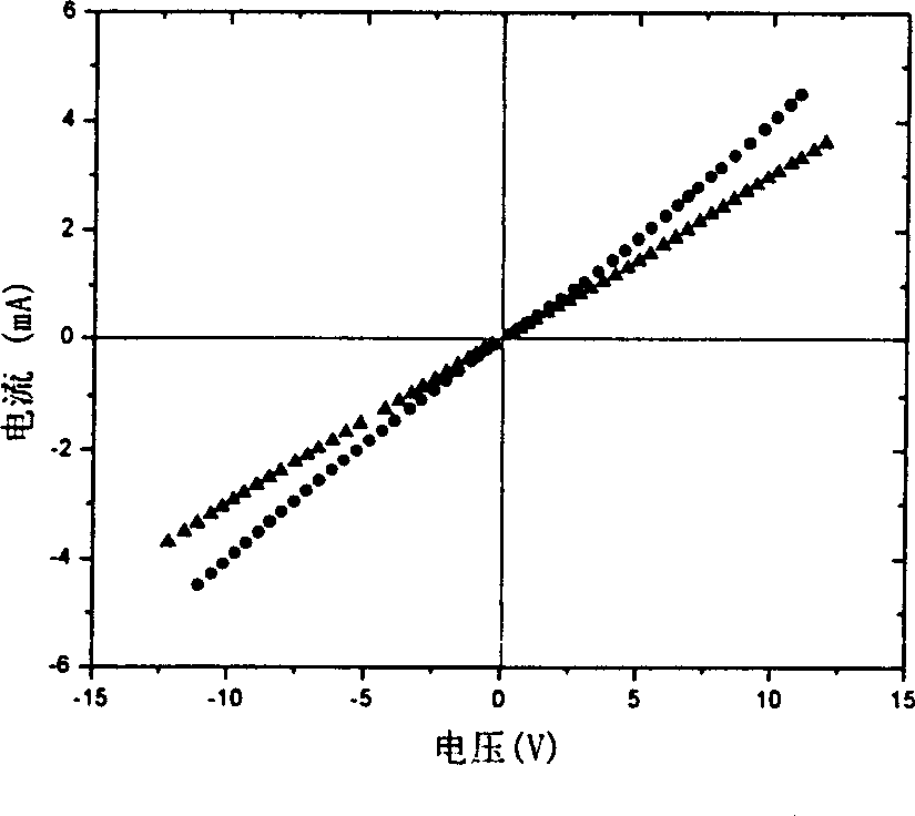
[0019] Example 2, on the low-resistance p-type ZnO, after evaporating Ni and Au, rapid thermal annealing is carried out at 300° C. or 400° C. in nitrogen for 150 seconds.

[0020] The p-type ZnO flakes were grown on sapphire (Al) by molecular beam epitaxy (MBE). 2 o 3 ) on nitrogen-doped low-resistance p-type ZnO, with an area of ​​about 1cm 2 , and its resistivity is about 4Ω·cm.

[0021] Firstly, the p-type ZnO sheet was cleaned by ultrasonic cleaning with acetone and absolute ethanol for 5 minutes; rinsed with deionized water and washed with dry N 2 blow dry. The thickness is 0.2mm and the area is 6×6cm 2 The tantalum sheet is used as a metal mask, and two areas of 1mm are formed on the tantalum sheet by machining. 2 The shape of the circular hole is used as the electrode, the distance between the two electrodes is 2mm, and the distance between the mask plate and the evaporation source is 12cm. Ni and Au are 99.99% pure. The vacuum degree during vacuum evaporation is...


PUM

PropertyMeasurementUnit
Areaaaaaaaaaaa
Resistivityaaaaaaaaaa

Abstract

The invention relates to a manufacture method for P-type ZnO ohim electrode, which comprises: depositing Ni on P-type ZnO with vacuum evaporation device to form the first layer of Ni electrode material; depositing Au to form the second Au layer of electrode material as electrode; taking rapid hot annealing to prepared electrode in nitrogen at low temperature to reduce potential barrier height between metal and semiconductor interface for the atom mutual diffusion and achieve ohim contact. This invention can improve greatly the ohim property and reliability of electrode.

Description


Claims


Application Information

Patent Timeline
Owner CHANGCHUN INST OF OPTICS FINE MECHANICS & PHYSICS CHINESE ACAD OF SCI
Learn More