Low-temperature bonding method for tin-coated nano porous copper

A nanoporous copper, low temperature bonding technology, applied in nanotechnology, nanotechnology, nanotechnology for materials and surface science, etc., can solve the problem that nanoporous copper is easy to oxidize, has high bonding temperature, and has no significant nanometer size effect. and other problems, to achieve the effect of facilitating the reaction process, reducing the bonding temperature, and reducing the residual thermal pressure

Inactive Publication Date: 2017-09-22
HUAZHONG UNIV OF SCI & TECH
View PDF9 Cites 5 Cited by
  • Summary
  • Abstract
  • Description
  • Claims
  • Application Information

AI Technical Summary

Problems solved by technology

[0004] Aiming at the above defects or improvement needs of the prior art, the present invention provides a method for low-temperature bonding of tin-coated nanoporous copper. By coating tin on the surface of the nanoporous copper structure, the nanoporous copper is easily oxidized and the nano-size effect is solved. Insignificant and high bonding temperature technical issues

Method used


Image

  • Low-temperature bonding method for tin-coated nano porous copper
  • Low-temperature bonding method for tin-coated nano porous copper

Examples


Embodiment 1

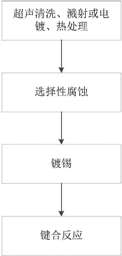
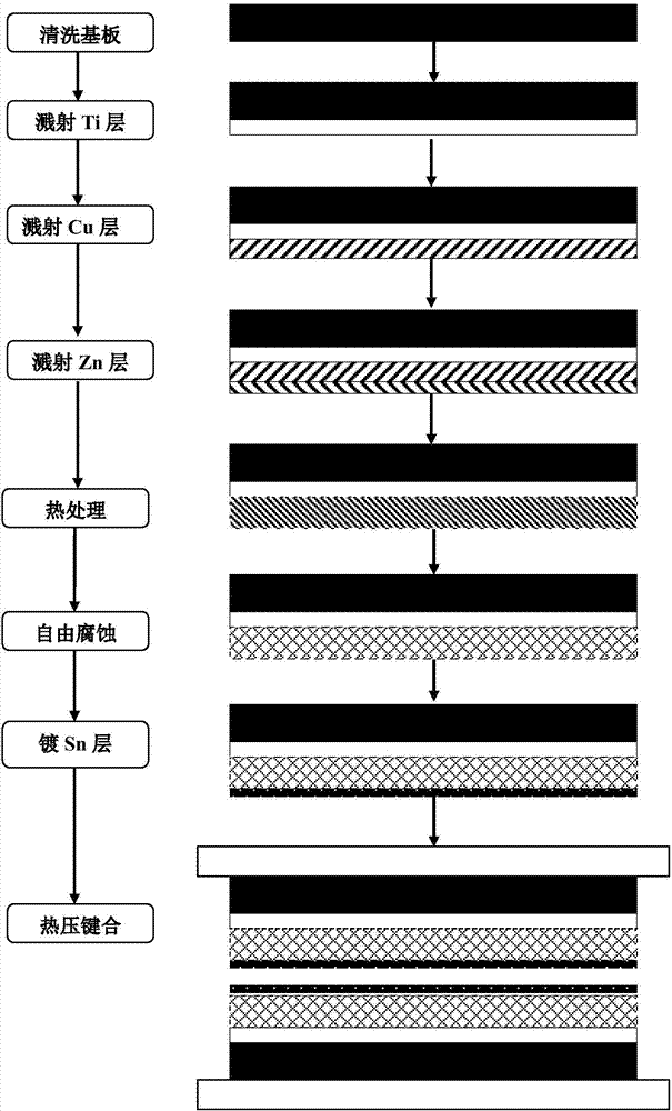
[0028] (1) Place the silicon wafer in a standard RCA cleaning solution for ultrasonic cleaning for 10 minutes, then sputter-deposit Ti layer (100nm), Cu layer (500nm) and Zn layer (1μm) in sequence, and then perform heat treatment (150°C, time 3h ) to obtain a Cu-Zn alloy layer.

[0029] (2) Place the above-mentioned silicon chip containing the Cu-Zn alloy layer in a NaOH solution with a concentration of 20%, and corrode it for 2 hours at a low temperature (-20° C.), remove the Zn element of the Cu-Zn alloy layer, and obtain on the surface of the silicon chip A nanoporous copper structure with a pore size of 20-30nm.

[0030] (3) Place the above-mentioned silicon wafer containing nanoporous copper in a tin plating solution, deposit tin on the surface of nanoporous copper by electroplating, the electroplating time is 20min, and the thickness of the tin layer is 300nm to obtain a tin-coated nanoporous copper structure.

[0031] (4) The above two silicon wafers containing tin-co...

Embodiment 2

[0033] (1) Place the aluminum nitride ceramic substrate in a standard RCA cleaning solution, clean it with ultrasonic waves for 10 minutes, then sputter and deposit a Ti layer (200nm) and a Cu layer (500nm) in sequence, electroplate a Zn layer (2μm), and then perform heat treatment (200°C, time 2h) to obtain a Cu-Zn alloy layer.

[0034] (2) Place the above-mentioned aluminum nitride ceramic substrate containing Cu-Zn alloy layer in 1% H 2 SO 4 In the solution, etch at room temperature for 2 hours, remove the Zn element in the Cu-Zn alloy layer, and obtain a nanoporous copper structure with a hole size of 60-80 nm on the surface of the aluminum nitride ceramic substrate.

[0035] (3) The above-mentioned aluminum nitride ceramic substrate containing nanoporous copper is placed in a tin plating solution, and tin is deposited on the surface of nanoporous copper by electroplating. The electroplating time is 30min, and the thickness of the tin layer is 1000nm to obtain tin-coated ...

Embodiment 3

[0038] (1) Clean the alumina ceramic substrate, then sputter-deposit Ti layer (100nm), Cu layer (500m) and Mg layer (1μm) in sequence, and then perform heat treatment (250°C, time 1h) to obtain Cu-Mg alloy layer.

[0039] (2) Place the above alumina substrate in a 1% tartaric acid solution, corrode it for 1 hour at a low temperature (-5°C), remove the Mg element of the Cu-Zn alloy layer, and obtain a pore size of 10-25nm on the surface of the alumina substrate nanoporous copper layer.

[0040] (3) The above-mentioned alumina ceramic substrate containing the nanoporous copper layer is placed in a tin plating solution, and a tin film is deposited on the surface of the nanoporous copper layer by electroless plating. The thickness of the tin plating layer is 800 nm, and the electroless plating time is 20 minutes.

[0041](4) Lay two aluminum oxide ceramic substrates whose surface is tin-coated nanoporous copper face to face, put them together on the hot plate of the bonding machin...


PUM

PropertyMeasurementUnit
diameteraaaaaaaaaa
thicknessaaaaaaaaaa
sizeaaaaaaaaaa

Abstract

The invention belongs to the field of electronic manufacturing, and discloses a low-temperature bonding method for tin-coated nano porous copper. The low-temperature bonding method comprises the steps of: firstly, preparing a copper alloy thin film on an initial substrate by means of ultrasonic cleaning, sputtering or electroplating, and thermal treatment; secondly, preparing a nano porous copper structure by adopting a selective corrosion process; thirdly, depositing tin on the surface of the nano porous copper structure to form a tin-coated nano porous copper structure; and utilizing the tin-coated nano porous copper structure as a bonding layer to realize bonding at low temperature and low pressure. The low-temperature bonding method is simple in process, can realize low-temperature and low-pressure bonding, serves at high temperature, reduces thermal stress generated by adopting the bonding process, and has wide application prospect.

Description

technical field [0001] The invention belongs to the field of electronic manufacturing, and more specifically relates to a method for low-temperature bonding of tin-coated nanoporous copper. Background technique [0002] With the increasing integration, miniaturization and multi-functionalization of electronic devices, Moore's Law is greatly challenged. The existing two-dimensional packaging is difficult to meet the technical requirements of packaging integration. Compared with two-dimensional packaging, three-dimensional packaging has the advantages of integration. At the same time, three-dimensional packaging can realize heterogeneous integration and reduce costs, making the product structure better and more diversified. Material bonding is the key to three-dimensional packaging It is one of the revolutionary technologies and seriously restricts the development of three-dimensional packaging technology. How to realize low-temperature bonding and high-temperature service is ...

Claims


Application Information

Patent Timeline
Patent Type & Authority Applications(China)
IPC IPC(8): H01L21/603H01L21/3213B82Y30/00
CPCB82Y30/00H01L21/3213H01L24/80H01L21/603
Inventor 陈明祥牟运李超
Owner HUAZHONG UNIV OF SCI & TECH
Why Eureka
Try Eureka