Polishing apparatus and polishing method

A technology for polishing devices and polishing surfaces, which is applied in the direction of grinding devices, electrical components, grinding machine tools, etc., and can solve the problems of polishing treatment application and influence

Active Publication Date: 2006-08-02
EBARA CORP
View PDF0 Cites 30 Cited by
  • Summary
  • Abstract
  • Description
  • Claims
  • Application Information

AI Technical Summary

Problems solved by technology

Because of the effect of the pad conditioning, the depth of the grooves formed in the surface of the polishing pad and the ratio of the soft lay...

Method used


Image

  • Polishing apparatus and polishing method
  • Polishing apparatus and polishing method
  • Polishing apparatus and polishing method

Examples


Embodiment Construction

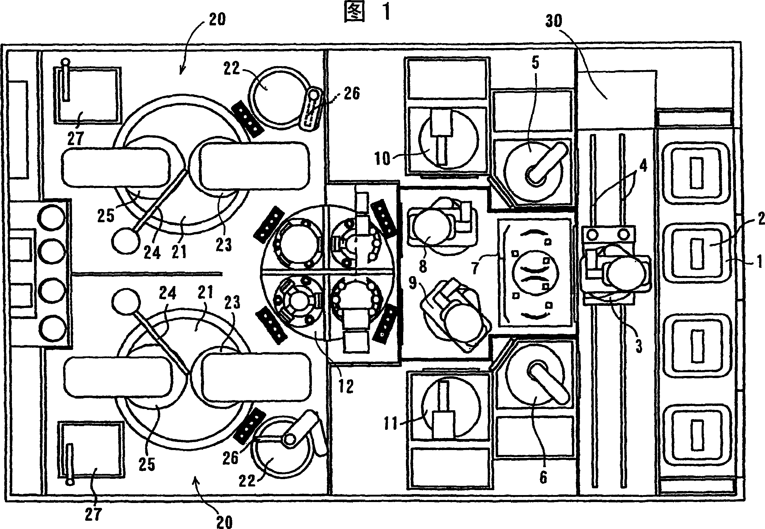
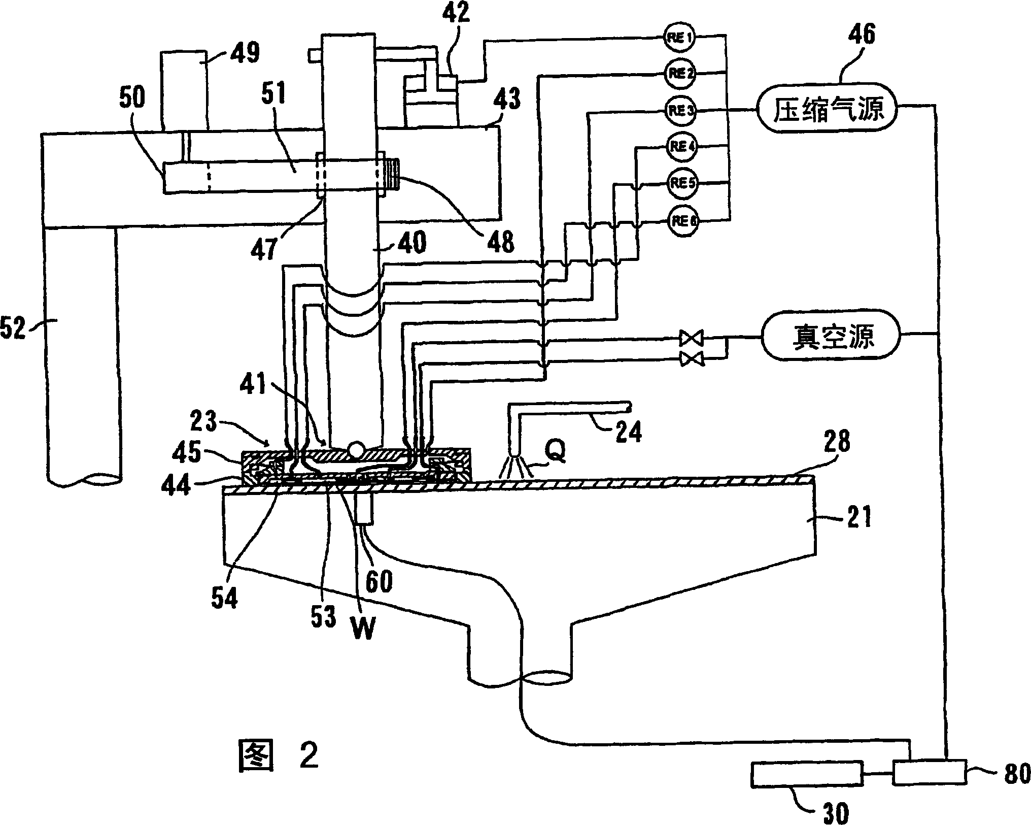
[0048] Reference will now be made to Figures 1 through Figure 13B A polishing apparatus according to an embodiment of the present invention will be described. In the respective drawings, the same or corresponding components are denoted by the same or corresponding reference numerals, and description thereof will not be repeated subsequently.

[0049] FIG. 1 is a plan view showing the overall structure of a polishing apparatus according to a first embodiment of the present invention. As shown in FIG. 1 , the polishing apparatus has four loading / unloading stations 1 each for receiving a cassette 2 containing (or storing) a plurality of substrates such as semiconductor wafers. The polishing device also has a transfer robot (manipulator) 3 which is arranged on a rail 4 so that the transfer robot 3 can move along the rail 4 to reach the corresponding cassette 2 on each loading / unloading station 1 . The polishing device also has two cleaning units 5 and 6 arranged on the opposite...


PUM


Abstract

A polishing apparatus is disclosed, comprising a polishing section configured to polish a substrate, wherein the substrate has a plurality of laminating films including an upper layer and a lower layer; a measurement section configured to measure a thickness of a film formed on the substrate; an interface configured to input a desired thickness of a film formed on a substrate to be polished; an arithmetic unit operable to calculate a polishing rate and an optimal polishing time based on the polishing rate data and the desired thickness by using a weighted average method which weights the polishing rate data on a lately polished substrate. The invention also discloses a polishing method.

Description

technical field [0001] The present invention relates to a polishing apparatus and a polishing method, and more particularly, to a polishing apparatus and a polishing method for polishing (grinding) a substrate such as a semiconductor wafer to a flat mirror finish. Background technique [0002] In recent years, semiconductor devices have become more integrated, and the structure of semiconductor elements has become more complicated. In addition, the number of layers in multilayer interconnect fabrics for logic systems has increased. Therefore, the unevenness on the surface of the semiconductor device is increased, so that the step height on the surface of the semiconductor device tends to become large. This is because, in the manufacturing process of a semiconductor device, a thin film is formed on the semiconductor device, then microprocessing such as forming a pattern or forming a hole is performed on the semiconductor device, and these processings are repeated to form a s...

Claims


Application Information

Patent Timeline
IPC IPC(8): H01L21/304B24B37/04B24B37/013
Inventor 佐佐木达也山田青史胜间田好文清水展津野成亮三谷隆
Owner EBARA CORP
Why Eureka
Try Eureka