Silicon-on-nothing metal-oxide-semiconductor field-effect-transistor and method for manufacturing the same

A technology of oxide semiconductors and field effect transistors, which is applied in the field of metal oxide semiconductor field effect transistors and its manufacturing, and can solve problems such as complex methods

Inactive Publication Date: 2006-09-20
KOREA ADVANCED INST OF SCI & TECH
View PDF0 Cites 10 Cited by
  • Summary
  • Abstract
  • Description
  • Claims
  • Application Information

AI Technical Summary

Problems solved by technology

The method is also complex

Method used


Image

  • Silicon-on-nothing metal-oxide-semiconductor field-effect-transistor and method for manufacturing the same
  • Silicon-on-nothing metal-oxide-semiconductor field-effect-transistor and method for manufacturing the same
  • Silicon-on-nothing metal-oxide-semiconductor field-effect-transistor and method for manufacturing the same

Examples


Embodiment Construction

[0045] The present invention will now be described in conjunction with preferred embodiments with reference to the accompanying drawings.

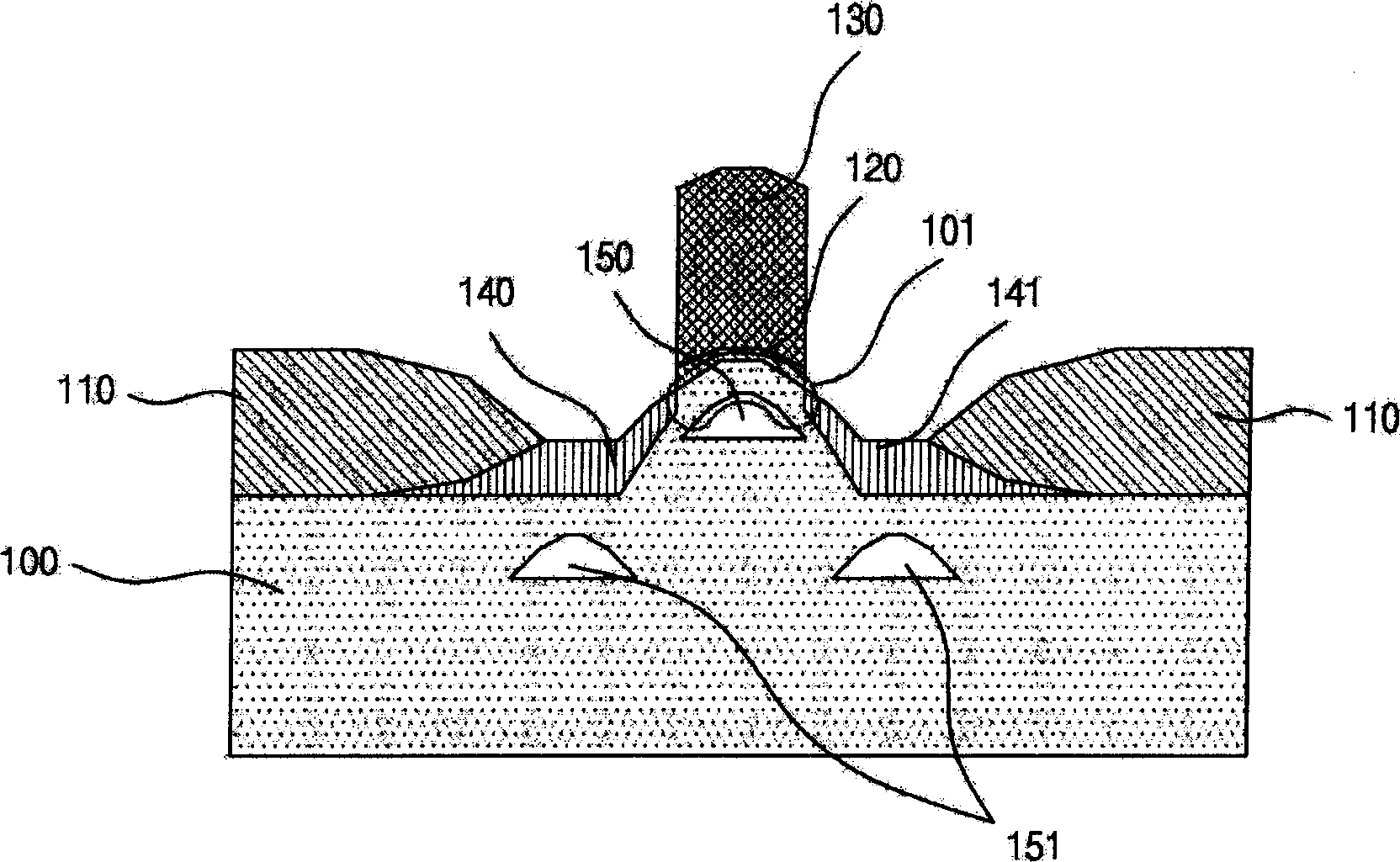
[0046] Refer to the following figure 2 A SON MOSFET according to one embodiment of the present invention is described. figure 2 is a cross-sectional view of a SON MOSFET according to one embodiment of the present invention.

[0047] refer to figure 2 , The SON MOSFET according to one embodiment of the present invention includes a silicon substrate 100, an isolation insulating film 110, a gate insulating film 120, a gate 130, a source region 140, a drain region 141, bubbles 150, 151 and a silicon channel 101.

[0048] Isolation insulating films 110 are formed on both sides of the top of the silicon substrate 100 . A gate insulating film 120 and a gate electrode 130 are sequentially stacked on the surface of the silicon substrate 100 between the isolation insulating films 110 . The isolation insulating film 110 is used to electrically...


PUM


Abstract

The present invention relates to a SON MOSFET and method of manufacturing the same, in which a blister is formed within a silicon substrate, thus improving the disadvantages of a bulk structure and a Silicon-On-Insulator (SOI) structure at the same time. The SON MOSFET according to the present invention comprises isolation insulating films formed at both upper sides of a silicon substrate, a gate insulating film and a gate electrode that are sequentially formed on a surface of the silicon substrate between the isolation insulating films, a source region and a drain region that are formed on the silicon substrate between the gate insulating film and the isolation insulating films, a blister formed within the silicon substrate under the gate insulating film, and a silicon channel, which is surrounded by the blister, the source region and the drain region, within the silicon substrate, wherein the blister is formed of hydrogen or helium ion.

Description

technical field [0001] The present invention relates to a metal-oxide-semiconductor field-effect transistor (MOSFET) of a suspended silicon layer (Silicon-On-Nothing) (SON) and a manufacturing method thereof, more particularly, to such a SON MOSFET and a manufacturing method thereof, wherein Bubbles are formed within the silicon substrate, thereby improving both the bulk structure and the defects of the silicon-on-insulator (SOI) structure. Background technique [0002] In order to reduce the price of semiconductor devices and enhance their performance, semiconductor devices have been integrated and simultaneously made smaller in accordance with Moore's law. As semiconductor devices continue to be highly integrated, several problems of deteriorating device characteristics arise. [0003] For example, due to high integration, not only the channel length of the field effect transistor is shortened to 100nm or less, but the potential of the channel is also controlled by the dr...

Claims


Application Information

Patent Timeline
Patent Type & Authority Applications(China)
IPC IPC(8): H01L29/78H01L21/336
CPCH01L29/66545H01L29/1037H01L29/0653H01L29/78696H01L21/263H01L29/78654H01L21/26506H01L29/0649H01L21/18
Inventor 崔梁圭张东润
Owner KOREA ADVANCED INST OF SCI & TECH
Why Eureka
Try Eureka