

Etching method for making chalcogenide memory elements
A chalcogenide, memory element technology, applied in the direction of electrical components, etc., can solve the problem of not providing the benefits of the invention, etc.
Inactive Publication Date: 2006-09-20
UNAXIS USA
View PDF1 Cites 0 Cited by
- Summary
- Abstract
- Description
- Claims
- Application Information
AI Technical Summary
Problems solved by technology
[0008] The prior art does not provide any of the benefits provided by the present invention
Method used
View moreImage
Smart ImageViewing Examples

Examples
Embodiment
[0035] System specification
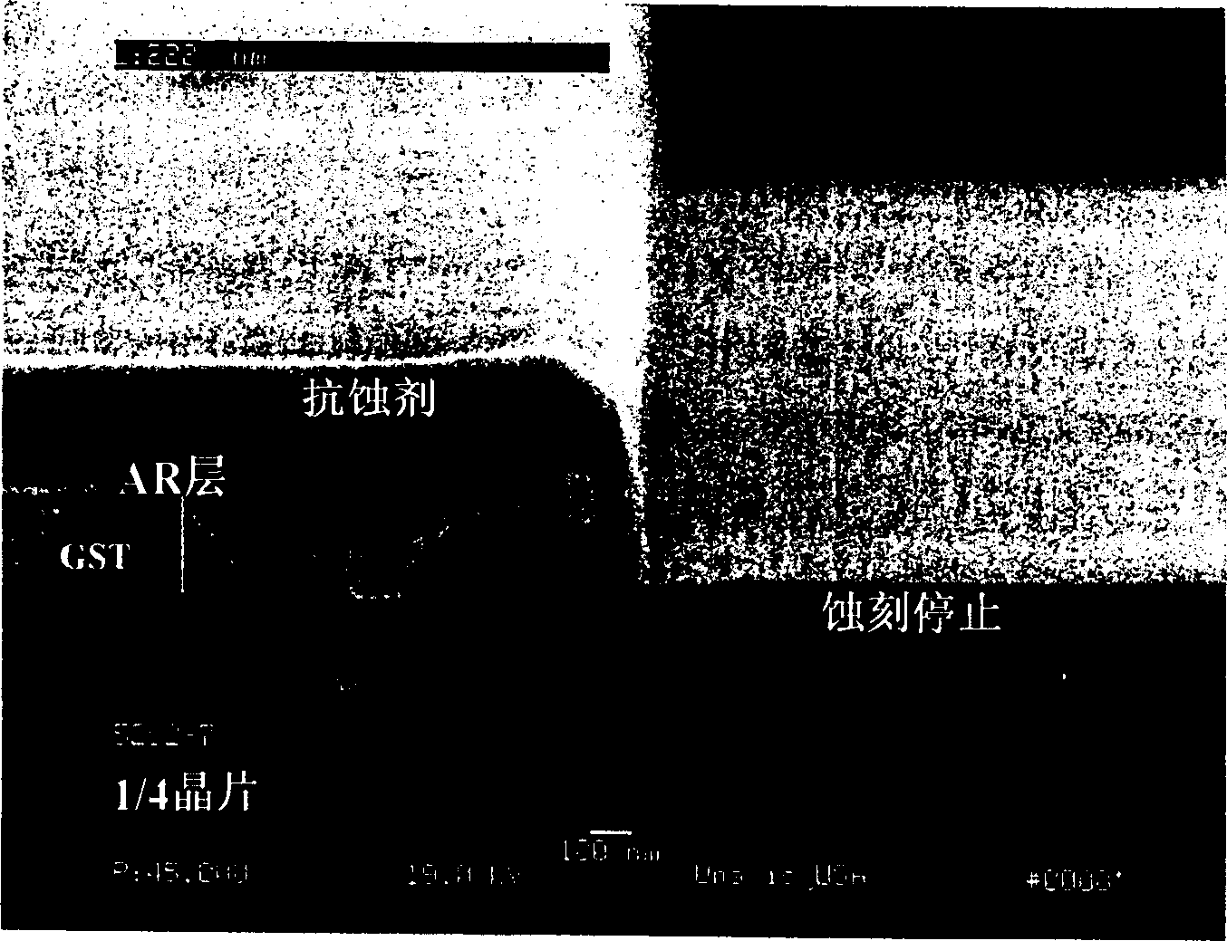
[0036] Initial experiments were performed on a commercial Unaxis SLR 770 etcher. The reactor used a 2MHz ICP source to generate a high density plasma. The ion energy at the substrate (wafer) was controlled by independently biasing the cathodes at 13.56 MHz. The wafer temperature was regulated by mechanically clamping the wafer to a liquid-cooled cathode combined with He backside cooling. End-of-process experiments used a commercial Unaxis Spectraworks Optical Emission System (OES).
Login to View More PUM
 Abstract
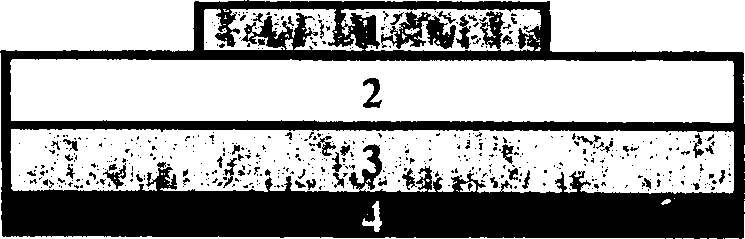
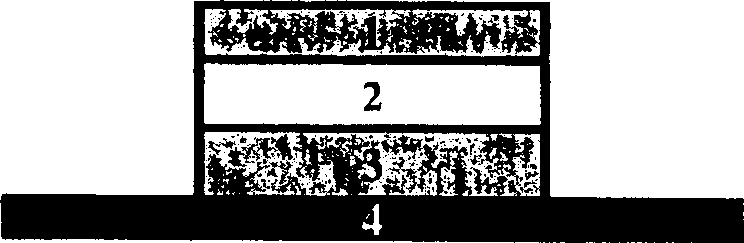
The present invention provides an improved method for forming a memory element having a chalcogenide layer such as Ge2Sb2Te5. A substrate having a dielectric etch stop layer, a chalcogenide layer, an anti-reflective layer and a mask layer is placed in a vacuum chamber having a high density plasma source. At least one chlorine containing gas, such as a mixture of BCl3 and Cl2, is introduced into the vacuum chamber for etching the chalcogenide layer and the anti-reflective layer to the dielectric etch stop layer. The etch process is discontinued based on an endpoint detection system. Upon completion of the etch process, the substrate is removed from the vacuum chamber and the mask layer is stripped from the substrate.
Description
[0001] This application is related to and claims priority to commonly owned US Provisional Patent Application No. 60 / 488,921, filed July 21, 2003, entitled "Plasma Etching of GeSbTe Films," which is incorporated by reference. technical field [0002] The present invention generally relates to the field of semiconductor devices and fabrication, and more particularly, the present invention relates to memory elements and methods of making memory elements. Background technique [0003] Chalcogenide material alloys have the ability to transform between amorphous and crystalline phases by applying temperature. The phase transition changes both the electrical and optical properties of the material. Recently, these materials have been introduced into non-volatile memory elements such as phase change memory (OUM). [0004] The common chalcogenide used to produce OUM is Ge x Sb y Te z (GST), where typical values are x=2, y=2 and z=5. With an input of picojoules of energy, the c...
Claims
Login to View More Application Information
Patent Timeline
 Patent Type & AuthorityApplications(China)
IPC IPC(8): H01L45/00
Inventor李耀升迈克·德夫雷
OwnerUNAXIS USA