Transmission platform for semiconductor wafer processing

A technology of wafer processing and transmission platform, applied in the direction of conveyor objects, transportation and packaging, etc., can solve the problems of limited number of wafers, difficult to improve production efficiency, etc., to achieve good compatibility, improve output rate, reduce the effect of exchange frequency

Active Publication Date: 2006-10-11
BEIJING NAURA MICROELECTRONICS EQUIP CO LTD
View PDF0 Cites 18 Cited by
  • Summary
  • Abstract
  • Description
  • Claims
  • Application Information

AI Technical Summary

Problems solved by technology

[0006] In the above transfer structure, one manipulator is responsible for the transfer of all wafers, the exchange of wafers in the vacuu...

Method used


Image

  • Transmission platform for semiconductor wafer processing
  • Transmission platform for semiconductor wafer processing
  • Transmission platform for semiconductor wafer processing

Examples


Embodiment Construction

[0025] The following examples are used to illustrate the present invention, but are not intended to limit the scope of the present invention. Those of ordinary skill in the relevant technical field can also make various changes and modifications without departing from the spirit and scope of the present invention. Therefore All equivalent technical solutions also belong to the category of the present invention, and the scope of patent protection of the present invention should be defined by each claim.

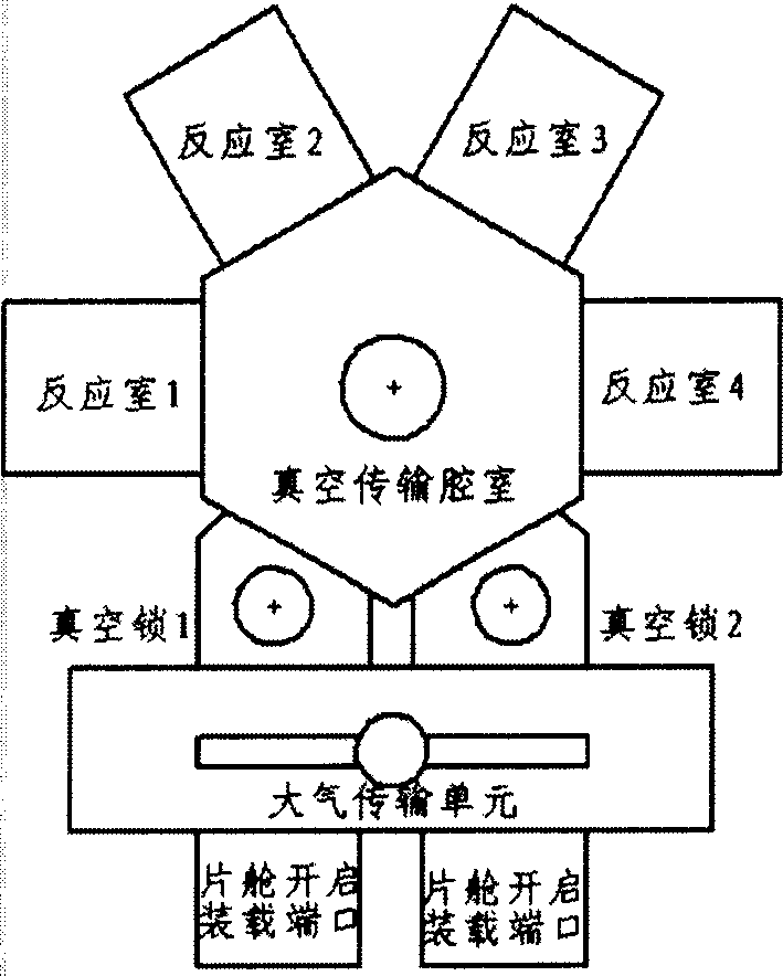
[0026] Such as Figure 5 As shown, a transmission platform for semiconductor wafer processing includes two wafer cabins with open loading ports, first to sixth reaction chambers, and an axisymmetric hexagonal structure vacuum transmission chamber, which adopts an axisymmetric non-regular hexagonal structure. Arrange two vacuum manipulators R1, R2 on the polygonal axis in the vacuum transfer chamber, and arrange two wafer temporary storage areas P1, P2 symmetrically perpendicul...


PUM


Abstract

The related transmission platform for a semiconductor wafer processing comprises: a port for wafer-cabin opening and loading, some reaction chambers, and a vacuum axisymmetrical polygonal transmission cavity. Wherein, arranging some vacuum manipulators, some wafer temporary areas, two vacuum locks on nearby polygonal edges, and the reaction chambers on other edges; applying the manipulators near the lock for transmission among the lock, nearest chamber and the temporary area, and other manipulators for transmission among the near areas and chambers. This invention has more wide application area and well compatibility.

Description

technical field [0001] The invention relates to semiconductor wafer processing equipment, in particular to a transmission platform for semiconductor wafer processing. Background technique [0002] During the processing of semiconductor wafers, the process reaction is carried out from the chip cabin to the reaction chamber. After the process is completed, the wafer is transferred from the reaction chamber back to the chip cabin. The vacuum transfer chamber is an important part of the wafer transfer process. The central nervous system of the transmission system, which acts as a transportation hub. The specific transfer process is as figure 1 shown. [0003] At present, most of the semiconductor 300mm adopts such as figure 2 , image 3 Structure. [0004] pass figure 2 It can be seen that the vacuum transmission chamber is a regular polygonal structure. The vacuum manipulator is located in the middle of the vacuum chamber. Two vacuum lock chambers and multiple process...

Claims


Application Information

Patent Timeline
IPC IPC(8): H01L21/677
Inventor 张之山
Owner BEIJING NAURA MICROELECTRONICS EQUIP CO LTD
Why Eureka
Try Eureka