Bipolar transistor and radio frequency amplifier circuit

一种双极型晶体管、高频放大的技术,应用在高频放大器、放大器组合等方向,能够解决高频特性恶化、高频电力损失变大、无法增大Vbe负反馈电压等问题,达到布线设计简单化、消除高频增益的降低、防止部件数的增加的效果

Inactive Publication Date: 2006-10-18
PANASONIC CORP
View PDF2 Cites 4 Cited by
  • Summary
  • Abstract
  • Description
  • Claims
  • Application Information

AI Technical Summary

Problems solved by technology

Therefore, if the gap 119 is lengthened, the base-emitter resistance 122 becomes larger, and the negative feedback voltage of Vbe can be increased, but on the other hand, the loss of high-frequency power increases, and the high-frequency characteristics deteriorate.
[0022] As mentioned above, Figure 5A , Figure 5B The problem with the conventional bipolar transistor 101 is that since a signal combining DC and RF is supplied to the base electrode 107, in order to improve high-frequency characteristics, it is necessary to reduce the base-emitter resistance 122, and therefore it is impossible to increase the Vbe. negative feedback voltage

Method used


Image

  • Bipolar transistor and radio frequency amplifier circuit
  • Bipolar transistor and radio frequency amplifier circuit
  • Bipolar transistor and radio frequency amplifier circuit

Examples


no. 1 approach

[0071] Figure 7A It is a cross-sectional view showing the structure of a bipolar transistor in the high-frequency amplifier circuit of the present embodiment. Figure 7B is a cross-sectional view of the structure of the transistor 1 of this embodiment, and the cross-sectional view along the dotted line a-a' in the figure is Figure 7A . But when Figure 7A The emitter wiring 20 is omitted. exist Figure 7A in, with Figure 5A The difference between the structural cross-sectional view of the conventional bipolar transistor 101 is that the DC terminal 3 to which a direct current (DC) bias is supplied and the RF terminal 4 to which a high frequency (RF) power is supplied are provided separately. That is, DC bias and RF power are supplied to the base layer 8 from different electrodes (respectively, the base electrode 6 for DC and the base electrode 7 for RF). The more essential difference is that the base electrode 6 for DC and the base electrode 7 for RF 7 is electrically ...

no. 2 approach

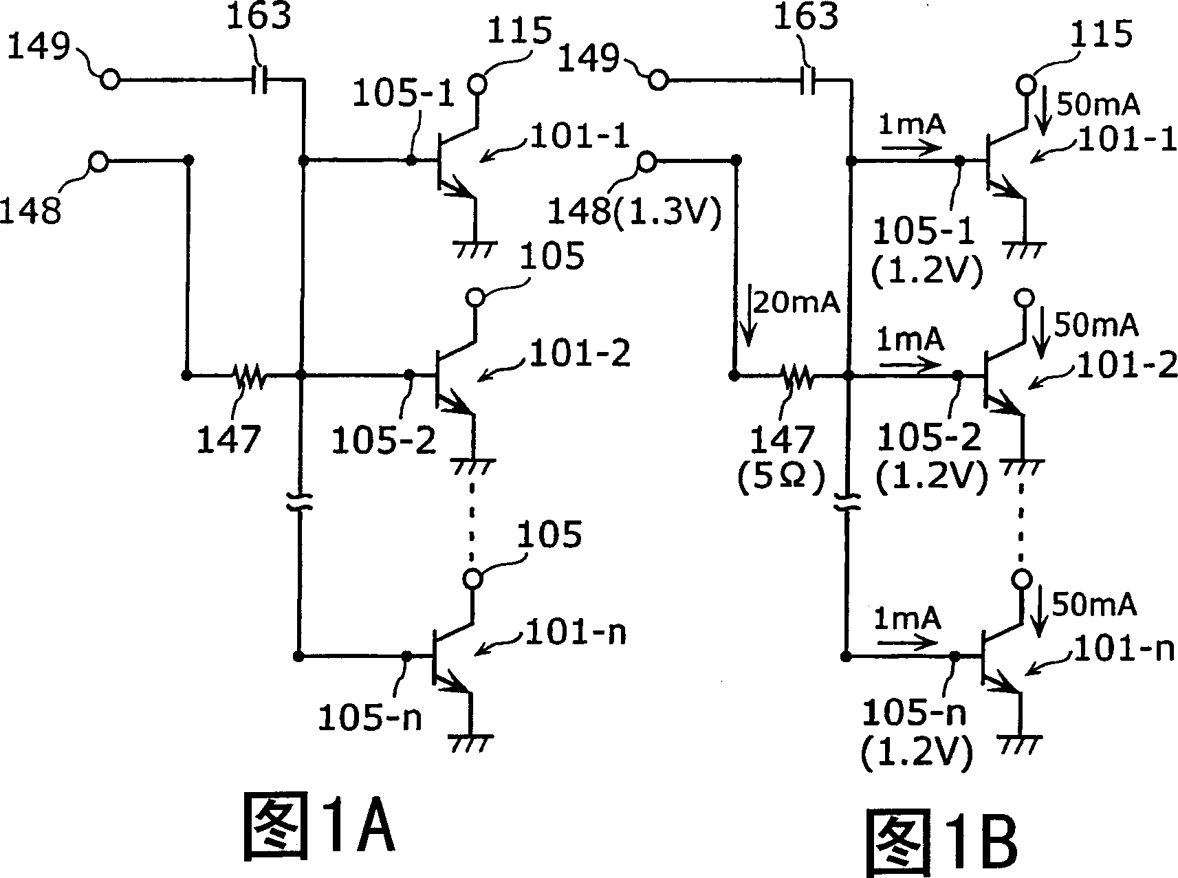
[0088] Next, in the first embodiment Figure 10 In the high-frequency amplifying circuit described in , it is considered that a collector current of 70 mA, which is 1.4 times that of other bipolar transistors, flows through the bipolar transistor 1-2. Such as Figure 11 As shown, the hFE of the bipolar transistors 1-1~1-n is 50, therefore, the base current flowing through the resistor 47-2 is 1.4mA, the voltage drop generated in the resistor 47-2 is 0.14V, and the electrode 6 The potential of -2 is 1.16V. On the other hand, the potential of the electrode 7-2 is 1.175V. At this time, the potential (1.175 V) of the electrode 7-2 is higher than the potential (1.16 V) of the electrode 6-2, so the base current of the bipolar transistor 1-2 is supplied from the electrode 7-2. That is, the negative feedback voltage of Vbe becomes 0.025V which subtracts 1.175V from 1.2V. On the other hand, the collector current of bipolar transistor 1-2 increases from 50mA to 70mA, whereby the jun...

no. 3 approach

[0096] Figure 14 It is a cross-sectional view of the structure of the bipolar transistor 70 in the high-frequency amplifier circuit of the third embodiment. with in Figure 12 The bipolar transistor 60 of the second embodiment shown is different in that it has a plurality of DC base electrodes 6-1, 6-2 and also has a plurality of emitter layers 11-1, 11-2. and Figure 12 Compared with the bipolar transistor 60, the emitter area is doubled, and the current capacity can be doubled in the unit cell. And, with Figure 12 Similarly, the bipolar transistor 60 is set to 3 μm by setting the distance from the DC base electrode 6-1 to the emitter layer 11-1 and the distance 61 from the DC base electrode 6-2 to the emitter layer 11-2. , the distance 16 from the RF base electrode 7 to the emitter layers 11-1, 11-2 is 0.5 μm, and Figure 12 The bipolar transistor 60 also, for any current concentration of the bipolar transistor, damage caused by thermal runaway of the bipolar transist...


PUM


Abstract

A bipolar transistor and a radio frequency amplifier circuit capable of preventing thermal runaway in the bipolar transistor without affecting the radio frequency amplifier circuit, which includes: a direct-current (DC) bias terminal to which a DC bias is supplied; a DC base electrode connected to the DC terminal; a radio frequency (RF) power terminal to which a radio frequency signal is supplied; an RF base electrode connected to the RF terminal; and a base layer connected to the DC base electrode and the RF base electrode.

Description

technical field [0001] The present invention relates to a semiconductor device, and more particularly, to a bipolar transistor and a high-frequency amplifier circuit including the bipolar transistor. Background technique [0002] Currently, in power amplifiers for mobile communications, GaAs-MESFET (Metal Semiconductor Field Effect Transistor, Metal Semiconductor Field Effect Transistor), GaAs-HEMT (High Electron Mobility Transistor, High Electron Mobility Transistor), heterojunction bipolar transistor (HBT: Hetero-iunction Bipolar Transistor) and the like. In particular, compared with GaAs-MESFET, the heterojunction bipolar transistor (hereafter, simply referred to as HBT) has the following advantages: (1) it does not require a negative power supply, so it can work with a single positive power supply; (2) it can increase Collector current density enables miniaturization of chip size. [0003] It is generally known that in bipolar transistors, if the temperature of the ele...

Claims


Application Information

Patent Timeline
Patent Type & Authority Applications(China)
IPC IPC(8): H03F3/189
CPCH03F3/19H03F3/68
Inventor 前田昌宏
Owner PANASONIC CORP
Why Eureka
Try Eureka