Thin-oxide devices for high voltage i/o drivers

A technology of output driver and output circuit, which is applied in the direction of logic circuit connection/interface layout, logic circuit coupling/interface using field effect transistors, etc., can solve problems such as excessive restrictions and complicated practical use of means, and achieve cost saving and manufacturing the effect of time

Active Publication Date: 2006-11-15
TAIWAN SEMICON MFG CO LTD
View PDF0 Cites 5 Cited by
  • Summary
  • Abstract
  • Description
  • Claims
  • Application Information

AI Technical Summary

Problems solved by technology

Although attempts have been made to solve this problem, the means of these

Method used


Image

  • Thin-oxide devices for high voltage i/o drivers
  • Thin-oxide devices for high voltage i/o drivers
  • Thin-oxide devices for high voltage i/o drivers

Examples


Embodiment Construction

[0024] In order to make the above-mentioned objects, features and advantages of the present invention more comprehensible, the following specific embodiments will be described in detail in conjunction with the attached figures.

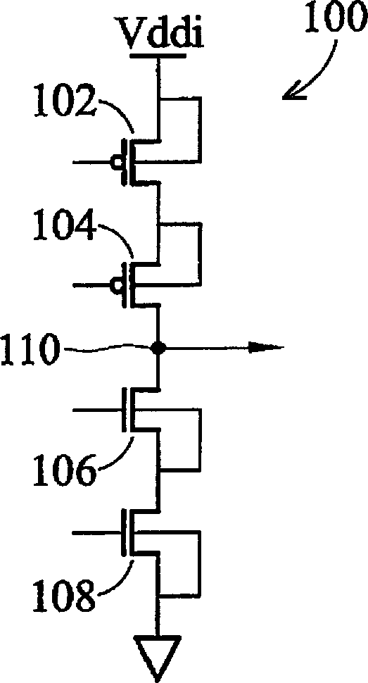
[0025] Figure 1A It is a schematic diagram showing an I / O driver 100 with thin oxide devices according to an embodiment of the present invention. I / O driver 100 is shown implemented using only thin oxide components. In this example, thin oxide PMOS transistors 102 and 104 along with thin oxide NMOS transistors 106 and 108 are arranged in series as a stack between an I / O power supply with I / O voltage (VDDI) and ground structure. The transistors 106 and 108 together act as a step-down module to pull the voltage on the output node 110 to a low potential. The transistors 102 and 104 are jointly used as a boost module to boost the voltage on the output node 110 to a high level. Its I / O voltage (VD DI ) is higher than a core voltage VDD C for core circui...


PUM


Abstract

An I/O driver includes a pull-down module and pull-up module. The pull-down module has one or more NMOS transistors serially coupled between ground and an output node. The pull-up module has one or more PMOS transistors serially coupled between a first voltage and the output node. The gates of the PMOS and NMOS transistors are controlled by a set of differential biases for selectively pulling the output node to the first voltage or ground. The differential biases are separately set for each of the transistors so that a voltage difference across each of the transistors does not exceed a predetermined value, thereby preventing the same from damage.

Description

technical field [0001] The present invention relates to integrated circuit design, and in particular to high voltage I / O (input / output) drivers (I / O drivers) without thick-oxide devices. Background technique [0002] Semiconductor technology is developing to extremely deep sub-micron geometries of less than 100 nanometers to more efficiently integrate more complex functions into a single chip. Although sub-100nm devices offer more complex functions and higher performance, they are also more expensive. [0003] It has been observed that when the channel length of a transistor is small enough, the current still exists due to the leakage current even in the standby state. Therefore, the supply voltage must be reduced relatively proportionally to minimize this leakage current. However, the I / O voltage of conventional I / O drivers is still maintained at a high voltage level such as 3.3V or 2.5V to be compatible with existing systems. In the prior art, thick oxide devices are co...

Claims


Application Information

Patent Timeline
IPC IPC(8): H03K19/0175H03K19/0185
Inventor 庄建祥
Owner TAIWAN SEMICON MFG CO LTD
Why Eureka
Try Eureka