Focusing ion beam modifying integrated circuit method and integrated circuit

A technology of focused ion beams and integrated circuits, applied in circuits, electrical components, electrical solid devices, etc., can solve problems such as bursting of non-metallic layers, electrostatic discharge, and inability to be guided away in time

Inactive Publication Date: 2007-01-03
VIMICRO CORP
View PDF0 Cites 1 Cited by
  • Summary
  • Abstract
  • Description
  • Claims
  • Application Information

AI Technical Summary

Problems solved by technology

During the hole digging step, when the channel passes through the non-metallic layer of the chip die, ions are easily gathered on the surface of the non-metallic layer on the inner wall of the channel, and cannot be guided away in time, resulting in electrostatic discharge. In severe cases, electrostatic discharge will Causes bursts of non-metallic layers to damage chips

Method used


Image

  • Focusing ion beam modifying integrated circuit method and integrated circuit
  • Focusing ion beam modifying integrated circuit method and integrated circuit

Examples


Embodiment Construction

[0023] The present invention will be further described in detail below in conjunction with the accompanying drawings and specific embodiments.

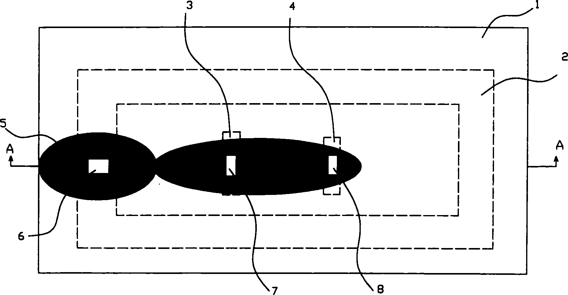
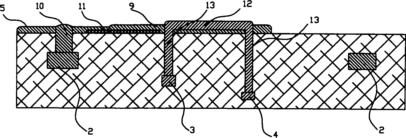
[0024] The core of the present invention is by laying a layer of grounded metal coating on the top layer of the integrated circuit (the said top layer refers to the initial layer of the digging of the integrated circuit), so that when carrying out FIB digging, the metal coating can be passed through Export the ions sputtered to the non-metallic surface to prevent the electrostatic discharge phenomenon from damaging the sample.

[0025] Based on this idea, this embodiment provides a method for modifying an integrated circuit with a focused ion beam, including a positioning step, a digging step and a deposition step.

[0026] Before the locating step or the digging step, the ground pin of the integrated circuit is grounded. The grounding method can adopt various existing methods in this technical field. In this embodiment, the pins of...


PUM


Abstract

The present invention discloses focusing ion beam modifying integrated circuit method. It contains positioning step, holing step and grounding ground wire pin of integrated circuit step, wherein positioning ground wire through hole and circuit wire through hole position in positioning step, plating first metal coating on ground wire through hole area of integrated circuit top layer before holing ground wire through hole, and depositing metal first metal coating in ground wire through hole, before holing circuit wire through hole plating first metal coating connected second metal coating on circuit wire through hole of integrated circuit, down holing circuit wire through hole to internal circuit wire of integrated circuit. The present invention also discloses modified integrated circuit adopting focusing ion beam.

Description

technical field [0001] The invention relates to an integrated circuit manufacturing process analysis and detection technology, in particular to a method for modifying integrated circuits by focused ion beams (Foucsed ion beams, FIB). [0002] The invention also relates to an integrated circuit processed by the method. technical background [0003] With the rapid development of integrated circuit technology, the integration level of chips has become higher and higher. However, high integration means that many smaller transistors and wires are gathered on a limited chip area, which puts forward higher requirements for the manufacturing process of integrated circuits. [0004] Focused ion beam FIB technology is usually compared to integrated circuit surgery, it can effectively analyze and detect integrated circuit manufacturing process, and carry out integrated circuit correction. [0005] The core of FIB technology is to use the high-energy ion beam focused by the electromag...

Claims


Application Information

Patent Timeline
Patent Type & Authority Applications(China)
IPC IPC(8): H01L21/70H01L27/02H01L23/60
Inventor 欧阳浩宇
Owner VIMICRO CORP
Why Eureka
Try Eureka