Thin film transistor substrate and manufacturing method thereof
A thin-film transistor and substrate technology, applied in the field of thin-film transistor substrate and its manufacture, can solve problems such as the loosening of the organic protective layer and the data pattern, reducing the adhesion between the photoresist and the data pattern, and pixel defects
- Summary
- Abstract
- Description
- Claims
- Application Information
AI Technical Summary
Problems solved by technology
Method used
Image

Examples
Embodiment Construction
[0041] Preferred embodiments of the present invention will be described below with reference to the accompanying drawings. In the drawings, the thickness of layers, films and regions are exaggerated for clarity of illustration. Like numbers indicate like elements throughout the figures. It will be understood that when an element such as a layer, film, region, or substrate is referred to as being "on" another element, it can be directly on the other element or intervening elements may also be present.
[0042] Although the channel of the thin film transistor applied to the present invention may be polysilicon, amorphous silicon a-Si, or other similar materials, only polysilicon thin film transistors and polysilicon thin film transistor substrates using polysilicon as channels will be described here.
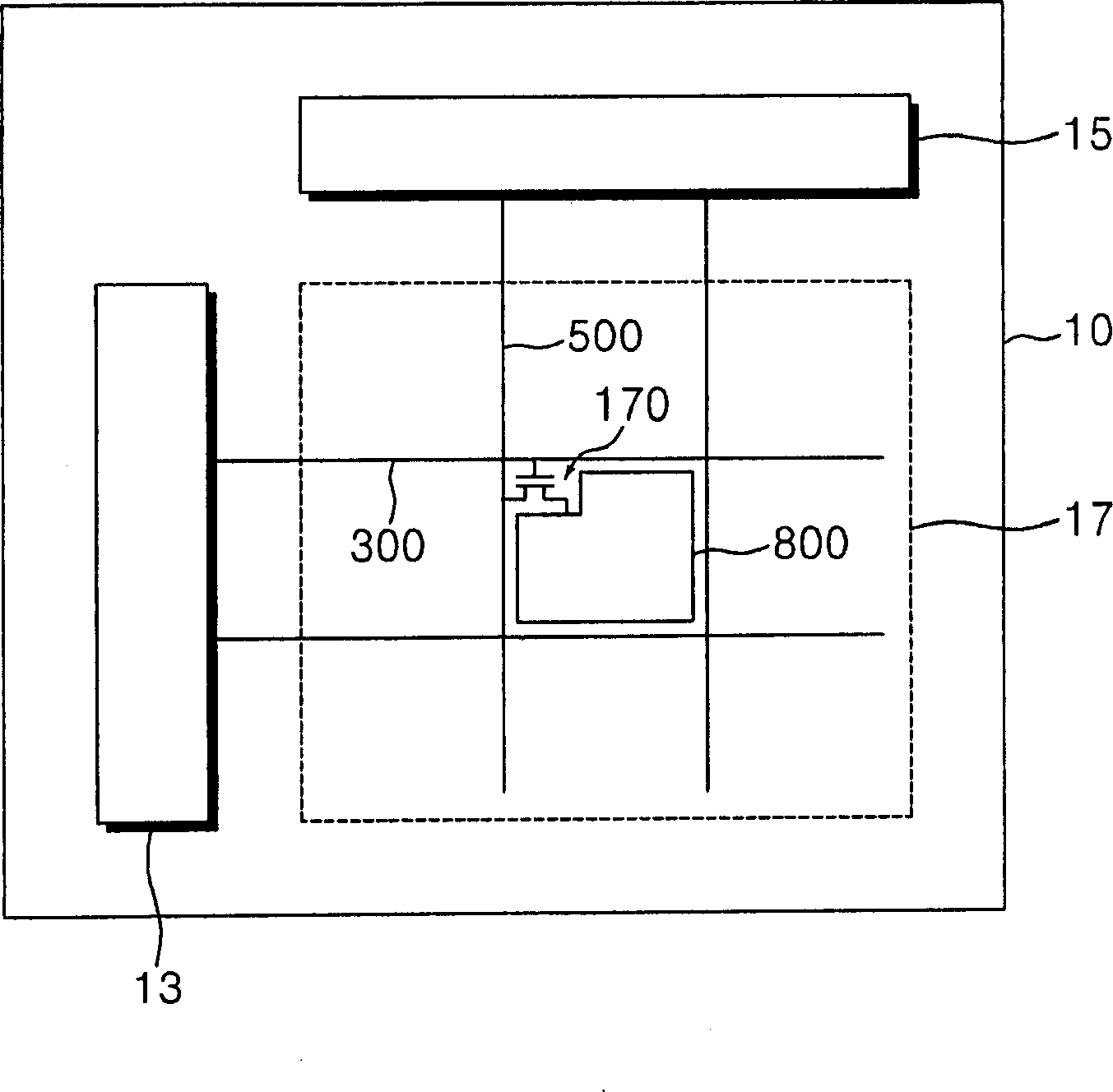
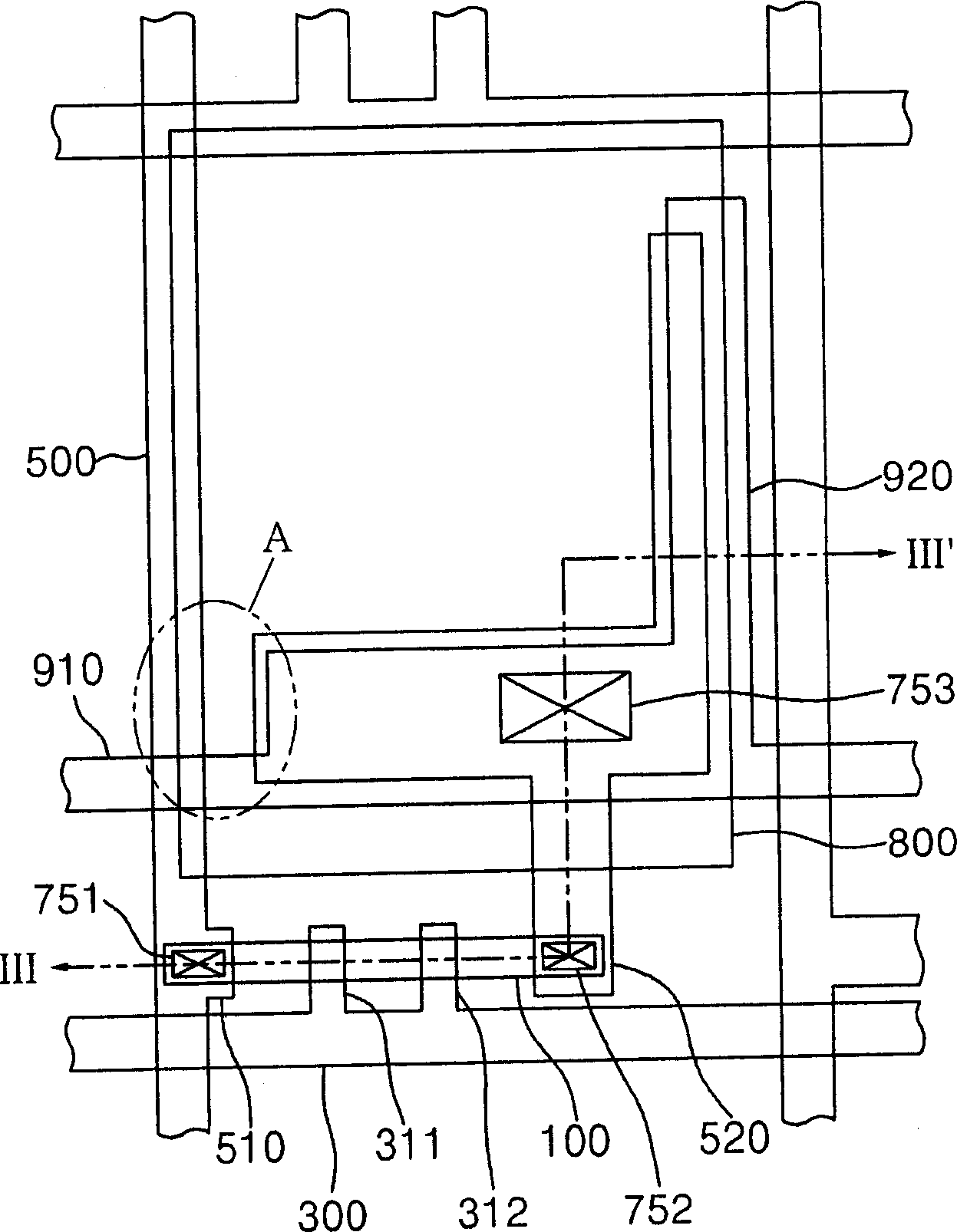
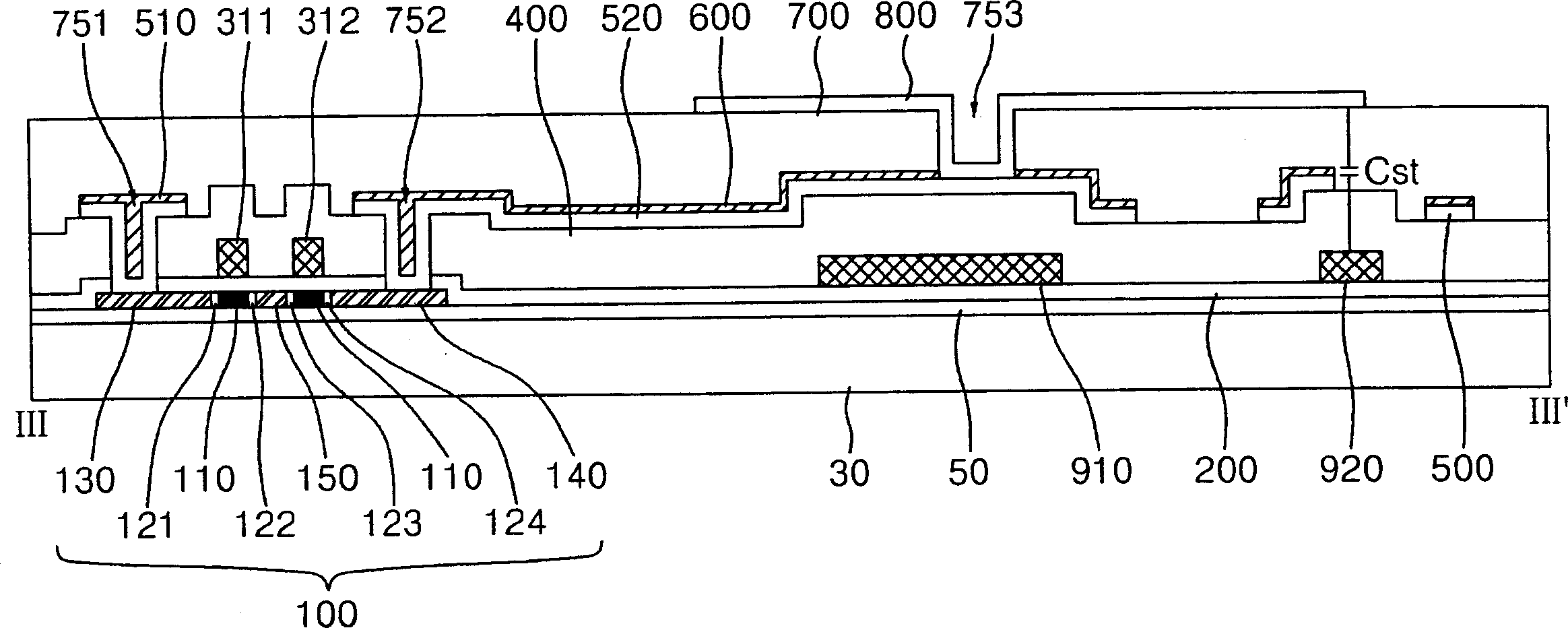
[0043] figure 1 is a layout diagram illustrating an exemplary embodiment of a thin film transistor substrate according to the present invention. figure 2 is the illustration ...
PUM
 Abstract
Description
Claims
Application Information
 - Generate Ideas
- Intellectual Property
- Life Sciences
- Materials
- Tech Scout
- Unparalleled Data Quality
- Higher Quality Content
- 60% Fewer Hallucinations
Browse by: Latest US Patents, China's latest patents, Technical Efficacy Thesaurus, Application Domain, Technology Topic, Popular Technical Reports.
© 2025 PatSnap. All rights reserved.Legal|Privacy policy|Modern Slavery Act Transparency Statement|Sitemap|About US| Contact US: help@patsnap.com