Optic scan module structure of scanning device

A scanning device and optical scanning technology, applied in image communication, electrical components, etc., can solve problems such as distortion, image quality degradation, and susceptibility to electromagnetic interference

Inactive Publication Date: 2007-01-24
AVISION PRECISION IND (SUZHOU) CO LTD
View PDF0 Cites 2 Cited by
  • Summary
  • Abstract
  • Description
  • Claims
  • Application Information

AI Technical Summary

Problems solved by technology

Taking the CCD of Sony ILX558K as an example, the number of input and output pins (pins) is as high as 12, which will increase the cost due to the large number of signal lines.
Moreover, since the optical analog signal RGB transmitted back from the CCD module 115 to the motherboard 150 is extremely susceptible to electromagnetic interference (Electromagnetic Interference, EMI), the optical analog signal RGB is likely to be distorted due to electromagnetic interference.
This will degrade the quality of the resulting image

Method used


Image

  • Optic scan module structure of scanning device
  • Optic scan module structure of scanning device
  • Optic scan module structure of scanning device

Examples


no. 1 example

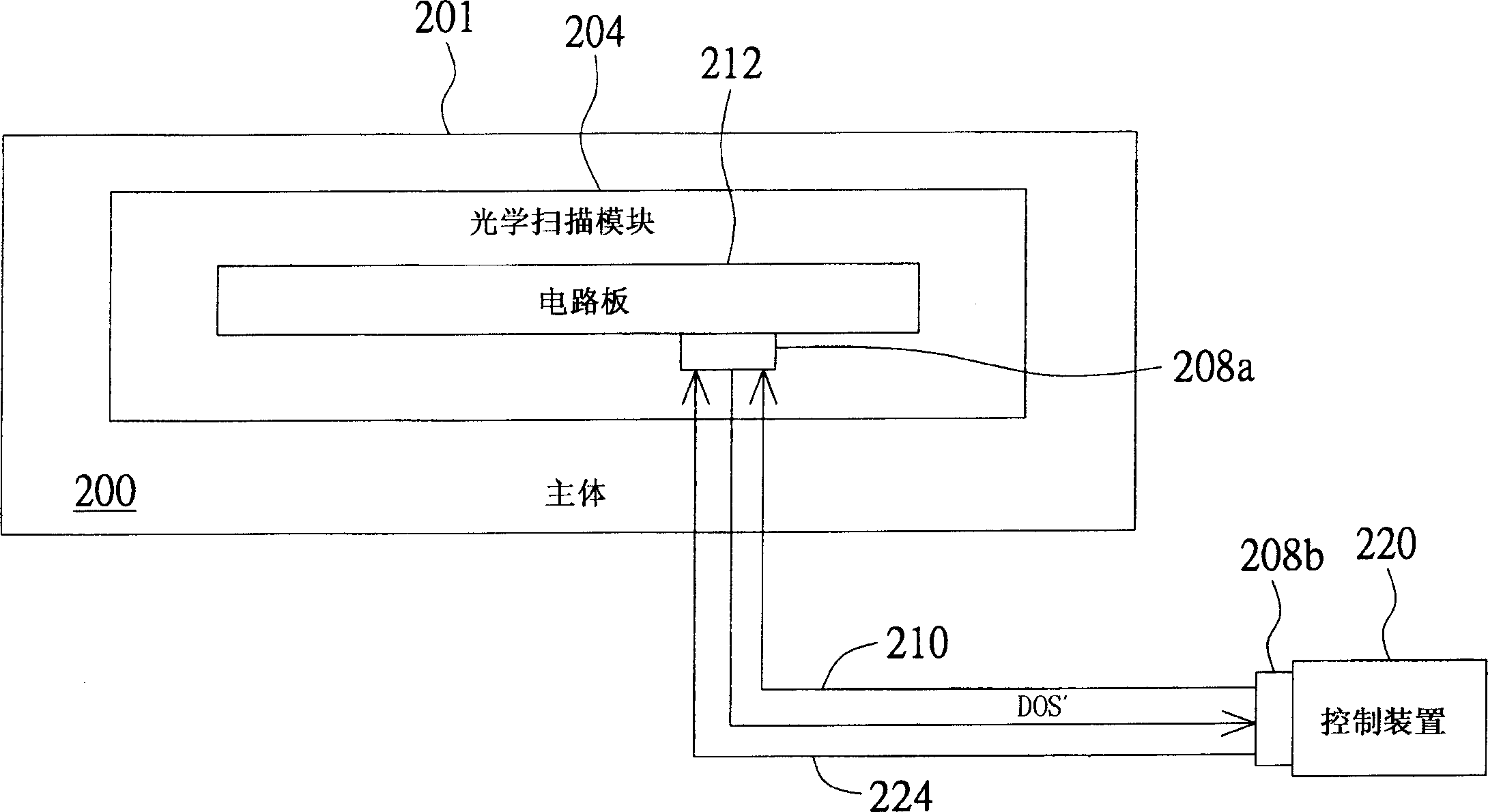
[0018] refer to image 3 , which shows a schematic diagram of the scanning device according to the first embodiment of the present invention. The scanning device 200 includes a main body 201 and an optical scanning module 204 . The optical scanning module 204 is configured on the main body 201 , and the optical scanning module 204 executes a scanning program under the control of the control device 220 . The control device 220 is a processor configured in the scanning device 200 or an external computer. A circuit board 212 is disposed on the optical scanning module 204 . The circuit board 212 is electrically connected to the control device 220 through the signal line 210 .

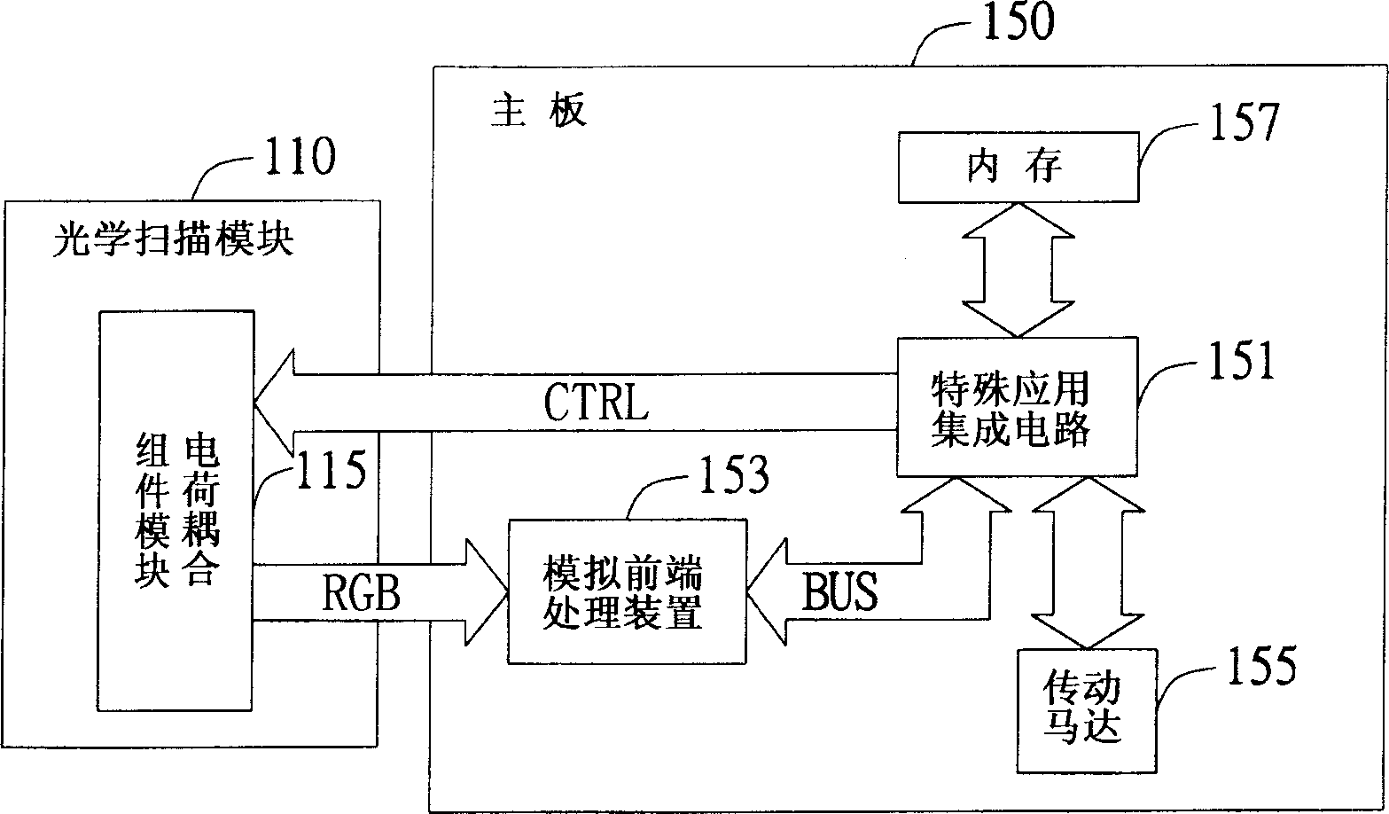
[0019] refer to Figure 4 , which shows a block diagram of a circuit configured on a circuit board according to the first embodiment of the present invention. The circuit board 212 is configured with a light sensing component 214 , a front-end processor 216 , an ASIC 218 and a transmission motor 222 . ...

no. 2 example

[0024] refer to Figure 5 , which shows a schematic diagram of a scanning device according to a second embodiment of the present invention. The scanning device 500 includes a main body 201 , an optical scanning module 204 , a power supply 206 and a bridge board 250 . The power supply 206 is configured on the main body 201 . The power supply 206 is disposed in the main body 201 , and the power supply 206 is used to provide the power required for the movement of the optical scanning module 204 . The optical scanning module 204 is configured on the main body 201 , and the optical scanning module 204 executes a scanning program under the control of the control device 220 . The bridge board 250 is configured at the interface of the scanning device 200 . The optical scanning module 204 is electrically connected to the control device 220 through the bridge board 250 and the signal line 210 . The bridging board 250 can be of RS-232, USB or IEEE1394 interface specification to be el...


PUM


Abstract

An optical scanning module is configured in a scanning device for picking up images of files including: an optical sensing component, a front processor and a special used IC, in which, the optical sensing component senses the optical signals of related files and converts the optical signals to analog image signals, a front processor is coupled with an optical sensing component and receives analog image signals and transforms them to digital image signals, the special application IC is used in receiving and processing digntal image signals and outputs them.

Description

technical field [0001] The invention relates to a scanning device, in particular to a scanning device which integrates a light sensing component, a front-end processor and a special application integrated circuit on an optical scanning module. Background technique [0002] refer to figure 1 , which illustrates a conventional scanner block diagram. The scanner includes two major image processing components, an optical scanning module 110 and a main board (Main Board) 150 fixed on the scanner body. The optical scanning module 110 is equipped with a Charge-Coupled Device (CCD) module 115 for receiving optical signal, while the application specific integrated circuit (Application Specific Integrated Circuit, ASIC) 151 and the analog front end (Analog Front End, AFE) processing device 153 on the motherboard 150 are used to control the charge-coupled device module 115, and the sensed The optical signal is extracted and converted to form an image signal tha...

Claims


Application Information

Patent Timeline
Patent Type & Authority Applications(China)
IPC IPC(8): H04N1/024
Inventor 林庆源
Owner AVISION PRECISION IND (SUZHOU) CO LTD
Why Eureka
Try Eureka