Display panel module

A display panel and printed circuit board technology, applied to static indicators, instruments, identification devices, etc., can solve the problems of reducing manufacturing pass rate and increasing production cost

Active Publication Date: 2007-02-07
AU OPTRONICS CORP
View PDF0 Cites 6 Cited by
  • Summary
  • Abstract
  • Description
  • Claims
  • Application Information

AI Technical Summary

Problems solved by technology

Therefore, the printed circuit board 120 must be approximately as long as the glass substrate of the display panel 110 so that it can be connected to all the data driving chips 112 correspondingly, which will increase the production cost and reduce the manufacturing yield.

Method used


Image

  • Display panel module
  • Display panel module
  • Display panel module

Examples


Embodiment Construction

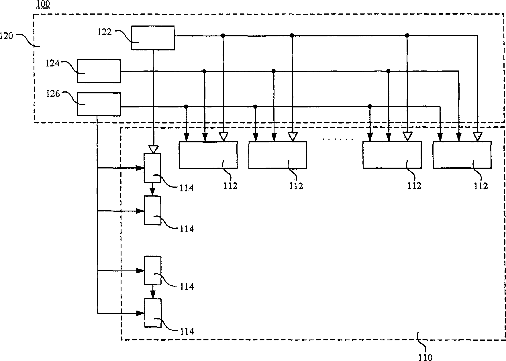
[0040] In the present invention, the data driving chips are arranged on the display panel in series, and at least two flexible printed circuit boards are used to transmit the data signal and the power signal respectively, so that the area of ​​the printed circuit board can be reduced to reduce the production cost. Furthermore, through the configuration of the relative positions between the data-driven chip and the flexible printed circuit board, the internal or external electrical connections between the signal contacts of the data-driven chip, etc., the present invention can further reduce the required flexible printed circuit board. The number of circuit boards is reduced, and the manufacturing yield is improved and the production cost is reduced.

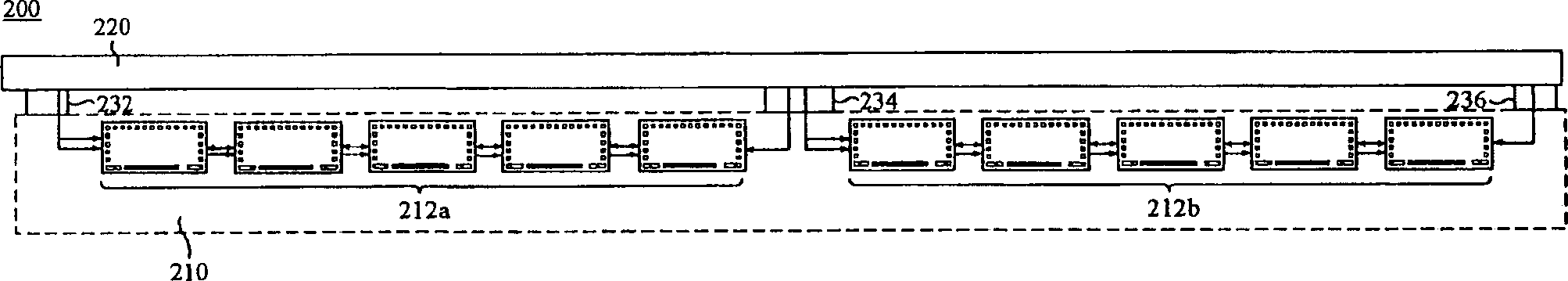
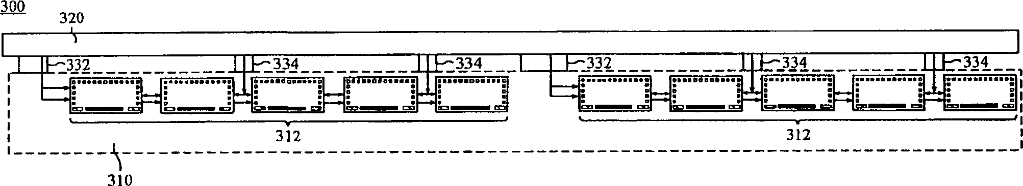
[0041] figure 2 A schematic diagram of a display panel module according to a preferred embodiment of the present invention is shown. The display panel module 200 includes a display panel 210, a printed circuit board 220, a firs...


PUM


Abstract

In the display panel, the data drive chip is connected on the panel in series, wherein the first flexible PCB is arranged between the PCB and one chip end to send data to the chip, and the second flexible PCB is arranged between the PCB and the chip to transmit power signal to the chip.

Description

technical field [0001] The invention relates to a flat display, in particular to a display panel module of the flat display. Background technique [0002] The driving method of the display panel is traditionally two flexible circuit boards (Tape Carrier Package; TCP) that are independently packaged with a data driver chip and a scan driver chip. Tape Automated Bonding (TAB) is respectively connected to the data lines and the scan lines of the display panel to drive multiple pixels of the display panel. With increasing demand for display panels and cost considerations, the current technology tends to omit the above-mentioned circuit board, such as directly attaching the driver chip on a glass substrate (Chip On Glass; COG). [0003] figure 1 A schematic diagram of a conventional display panel module 100 is shown. The data driver chip 112 and the scan driver chip 114 are directly attached on the glass substrate of the display panel 110 using chip on film (COF) technology. ...

Claims


Application Information

Patent Timeline
Patent Type & Authority Applications(China)
IPC IPC(8): G09G3/20G09F9/30
Inventor 许胜凯杨智翔
Owner AU OPTRONICS CORP
Why Eureka
Try Eureka