Organic light-emitting device having improved stability
A device, organic layer technology, applied in the field of top- and bottom-emitting organic light-emitting diodes, which can solve the problem of energy waste
- Summary
- Abstract
- Description
- Claims
- Application Information
AI Technical Summary
Problems solved by technology
Method used
Image
Examples
Embodiment 1
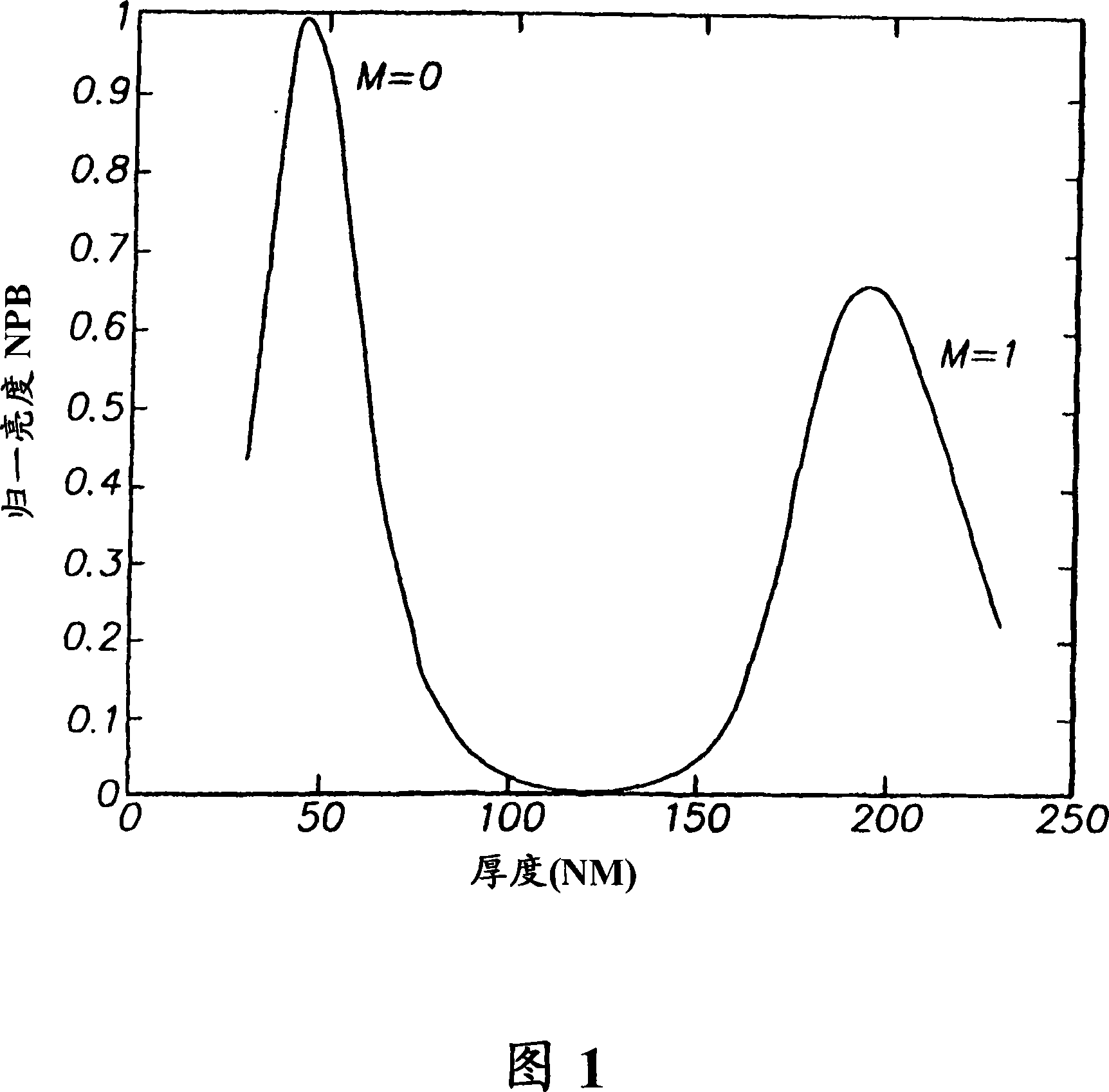
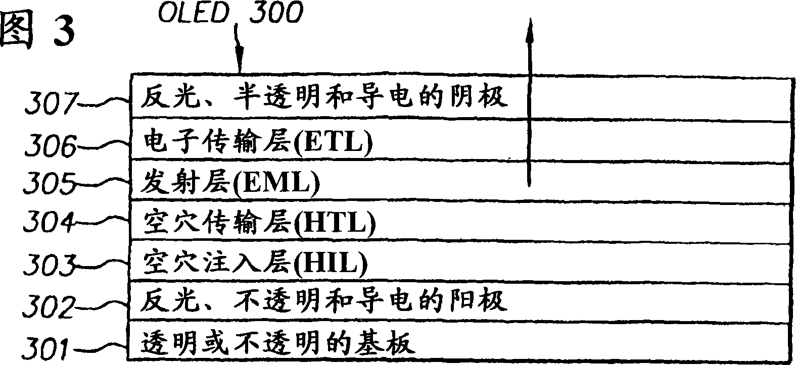
[0079] The prior art top-emitting device OLED 1A and the inventive top-emitting device OLED 1B were produced in the same procedure. Whereas the prior art devices were fabricated on glass substrates containing a 60 nm thick pure Ag anode, the OLEDs of the present invention are bilayer anodes. The double-layer anode includes a 60nm thick pure Ag bottom layer and a 6nm thick AgMo alloy surface layer. The concentration of Mo in the surface layer was 20% by volume. Commonly used CF for each substrate deposition x HIL, NPB HTL, AlqEML / ETL and translucent top cathode. The cathode is a 14 nm thick translucent MgAg alloy. The concentration of Ag in the cathode layer was 10% by volume. This OLED structure was selected based on an opaque, totally reflective and single-layer pure Ag anode and optimized for maximum top emission. The device has the following layer structure:
[0080] OLED 1A: Glass(1.1mm) / Ag(60nm) / CF x (1nm) / NPB(45nm) / Alq(60nm) / MgAg(14nm)
[0081] OLED 1B: Glass(1....
Embodiment 2
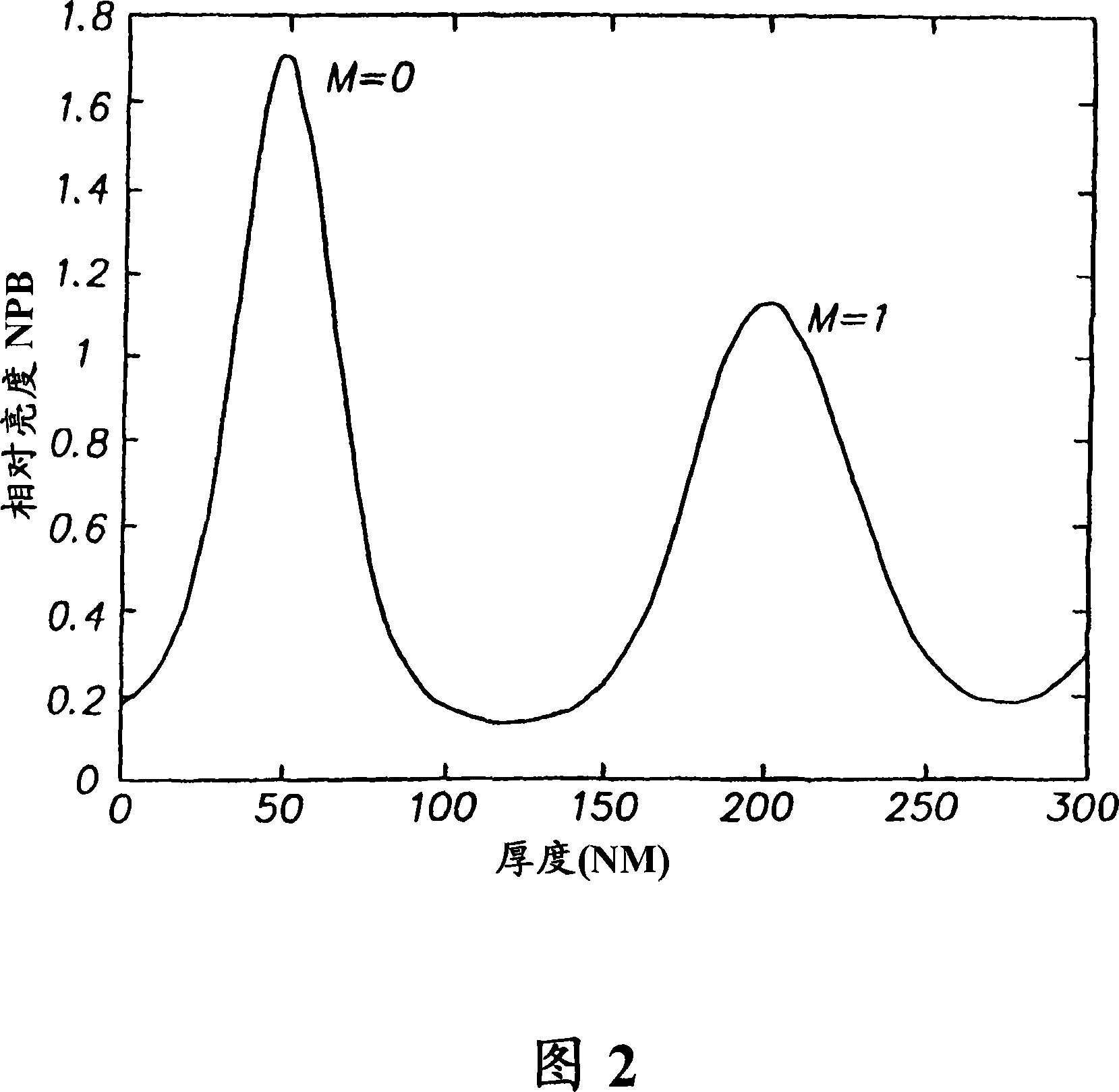
[0086] The bottom-emitting device OLED 2A of the prior art and the bottom-emitting device OLED 2B of the present invention were prepared in the same coating process. Whereas prior art OLEDs were fabricated on glass substrates containing a 20 nm thick translucent pure Ag anode, the OLED of the present invention is a double layer anode. The double-layer anode is also translucent, consisting of a 15nm thick pure Ag bottom layer and a 6nm thick AgMo alloy top layer. The concentration of Mo in the surface layer was 20% by volume. Commonly used CF for each substrate deposition x Top cathode for HIL, NPB HTL, Alq EML / ETL and total reflection. The cathode was an opaque MgAg alloy 220 nm thick. The concentration of Ag in the cathode layer was 10% by volume. The selection of this OLED structure was based on a semi-transparent, reflective and single-layer pure Ag anode and optimized to maximize bottom emission. The device has the following layer structure:
[0087] OLED 2A: Glass(1....
Embodiment 3
[0093] The bottom-emitting device OLED 3A of the prior art and the top-emitting device OLED 3B of the present invention were prepared in the same coating process. Whereas prior art OLEDs were fabricated on glass substrates containing a 20 nm thick translucent pure Ag anode, the OLED of the present invention is a double layer anode. The double-layer anode of the OLED of the present invention is opaque, including a 75nm thick pure Ag bottom layer and a 10nm thick AgMg alloy surface layer. The concentration of Mg in the surface layer is 50% by volume. Commonly used MoO for each substrate deposition x HIL, NPB HTL and Alq EML / ETL. The cathode of existing device 3A is a 100 nm thick fully reflective LiF / Al layer. The cathode of device 3B was a 14 nm thick translucent MgAg alloy. The concentration of Ag in the cathode layer was 10% by volume. The device has the following layer structure:
[0094] OLED 3A: Glass(1.1mm) / Ag(20nm) / MoO x (2nm) / NPB(200nm) / Alq(60nm) / LiF(0.5nm) / Al(1...
PUM
| Property | Measurement | Unit |
|---|---|---|
| electron work function | aaaaa | aaaaa |
| reflectivity | aaaaa | aaaaa |
| reflectivity | aaaaa | aaaaa |
Abstract
Description
Claims
Application Information


