Semiconductor memory and method for manufacturing the same
一种存储装置、制造方法的技术,应用在半导体/固态器件制造、半导体器件、电固体器件等方向,能够解决开口面积小、UV光入侵、存储器单元Vt升高等问题,达到可靠性高的效果
- Summary
- Abstract
- Description
- Claims
- Application Information
AI Technical Summary
Problems solved by technology
Method used
Image

Examples
Embodiment approach 1
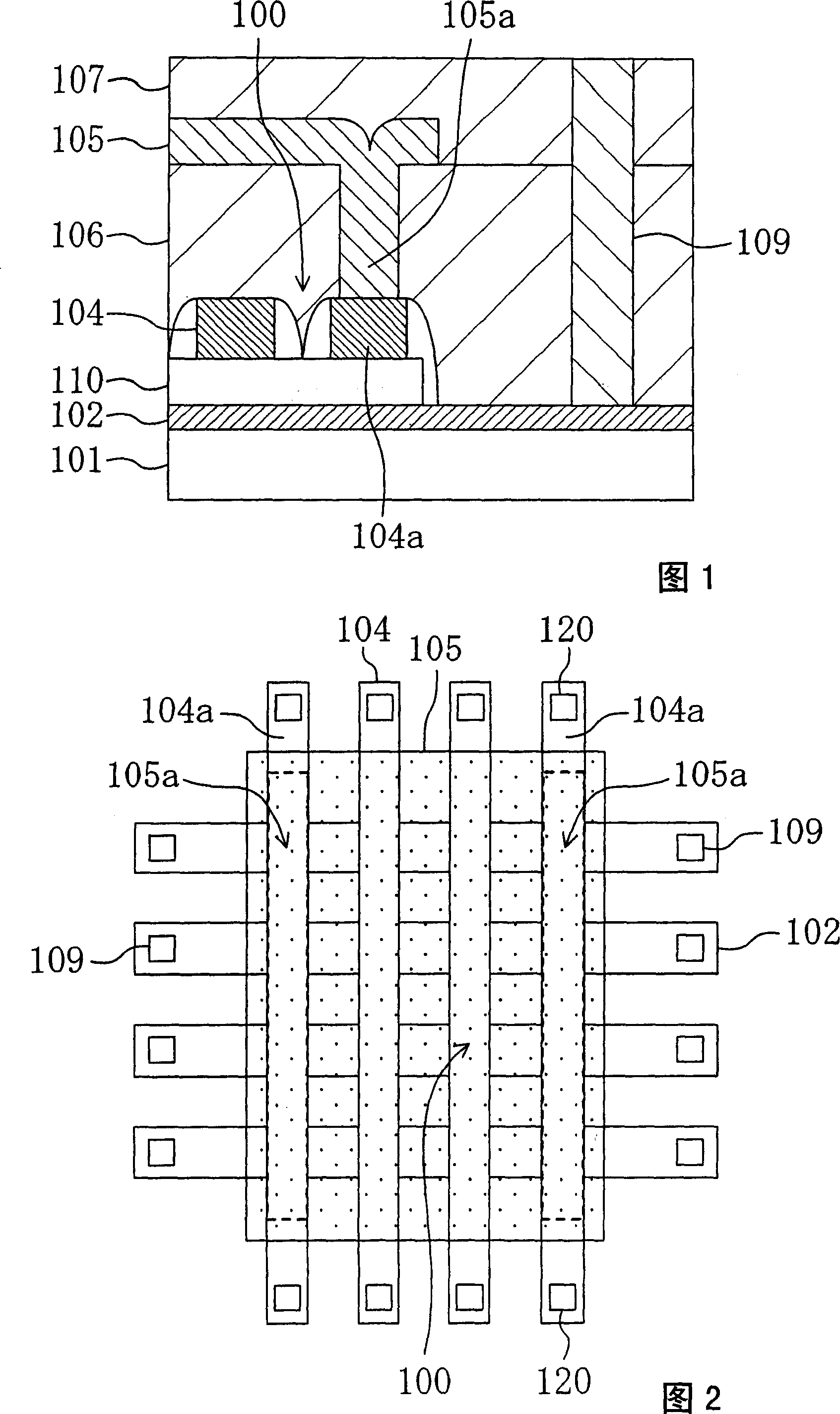
[0102] 1 is a cross-sectional view schematically showing the structure of a semiconductor memory device according to Embodiment 1 of the present invention, and shows the structure near a bit line contact post 109 .
[0103] As shown in FIG. 1 , the memory cell 100 is composed of bit lines 102 formed of a diffusion layer formed on a semiconductor substrate 101, and trapping gate insulating films (not shown) formed between the bit lines 102. ) and word lines 104 formed on the gate insulating film. Furthermore, an interlayer insulating film 106 is formed on the memory cell 100, and in the interlayer insulating film 106, a bit line contact post 109 connected to the bit line 102 is formed.
[0104] In addition, a light-shielding film 105 is formed on the interlayer insulating film 106 at least in a region covering the memory cell 100, and a part of the light-shielding film 105 formed on the interlayer insulating film 106 is formed in the vicinity of the bit line contact pillar 109,...
Embodiment approach 2
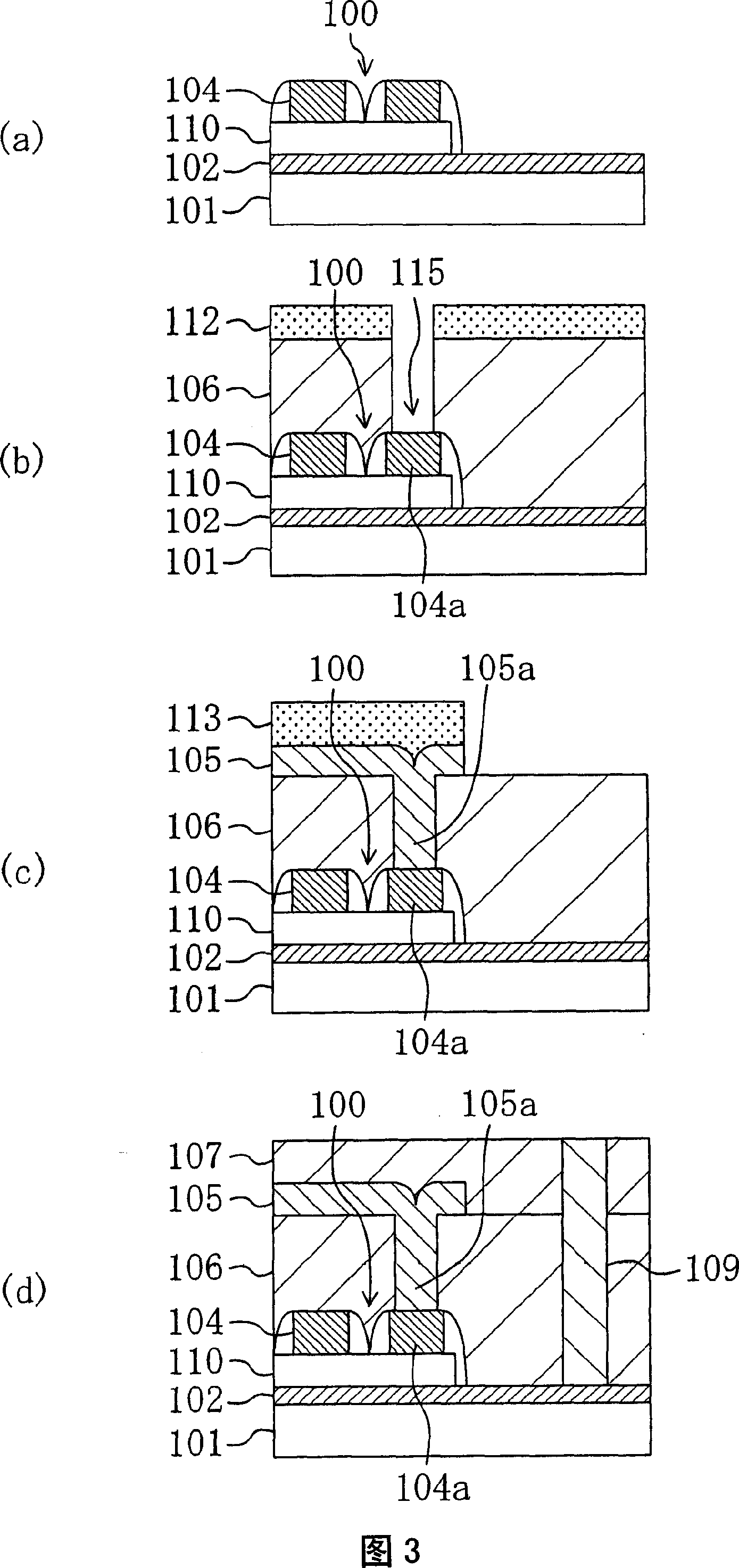
[0142] In the semiconductor memory device according to Embodiment 1 shown in FIG. 1, the light-shielding film 105 formed by extending into the interlayer insulating film 106 is formed parallel to the word line 104. As shown in FIG. The UV light intruding into the memory cell 100 is directed towards the side near the contact pillar 109 .
[0143] However, since the distance between the bit line contact stud 109 and its adjacent word line is generally shorter than the distance between the word line contact stud 116 and its adjacent bit line 102, it prevents contact from the bit line contact stud 109. The UV light intruding into the memory cell 100 from the side near the word line is more effective than the UV light intruding into the memory cell 100 from the side near the word line contact pillar 116 . Therefore, the structure of the light-shielding film 105 shown in Embodiment Mode 1 can be said to be an extremely effective means for improving the reliability of the semiconduct...
Embodiment approach 3
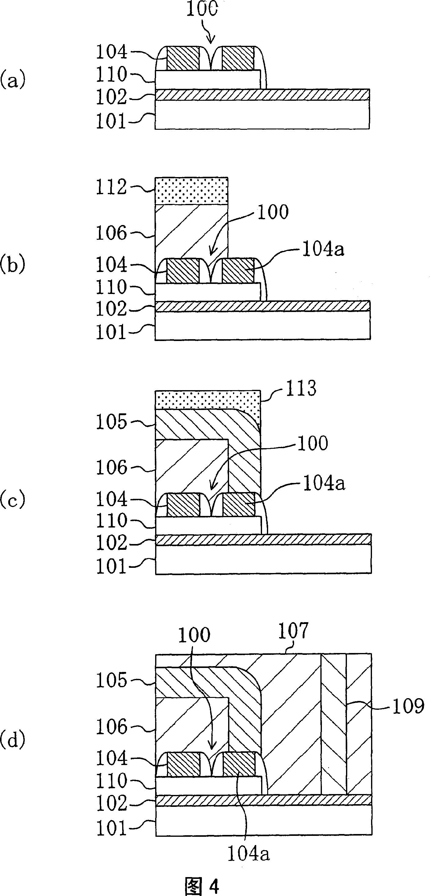
[0163] In the semiconductor storage device according to the second embodiment shown in FIGS. UV light intrusion into the memory cell 100 from the vicinity of the bitline contact pillar 109 and the vicinity of the wordline contact pillar 116 is blocked.
[0164] However, in the steps shown in FIG. 8(b) and FIG. 9(b), it is preferable to form the opening 115 formed in the interlayer insulating film 106 as close as possible to the word line 104, but since the opening 105 is formed by Since the interlayer insulating film 106 is etched by time, it is difficult to control the depth of the opening 115 without variation.
[0165] Therefore, in the third embodiment, a semiconductor memory device is proposed in which the depth of the light-shielding film 105 formed by extending in the interlayer insulating film 106 is well controlled. Next, it demonstrates concretely with reference to FIG. 10 (a), (b). In addition, detailed descriptions of the configurations common to the configuratio...
PUM
 Abstract
Description
Claims
Application Information
 - R&D
- Intellectual Property
- Life Sciences
- Materials
- Tech Scout
- Unparalleled Data Quality
- Higher Quality Content
- 60% Fewer Hallucinations
Browse by: Latest US Patents, China's latest patents, Technical Efficacy Thesaurus, Application Domain, Technology Topic, Popular Technical Reports.
© 2025 PatSnap. All rights reserved.Legal|Privacy policy|Modern Slavery Act Transparency Statement|Sitemap|About US| Contact US: help@patsnap.com