
Pulse shaping circuit

A pulse shaping and circuit technology, which is applied in the field of circuits where peaking is added to the pulse edge, can solve the problems of unfavorable high-speed applications, inability to distinguish the rising and falling edges of driving electrical pulses, and large turn-on pulses.

Active Publication Date: 2007-05-16
LUMENTUM OPERATIONS LLC
View PDF6 Cites 13 Cited by
  • Summary
  • Abstract
  • Description
  • Claims
  • Application Information

AI Technical Summary

Problems solved by technology

[0004] [4] The time delay associated with laser or LED switching on or off is detrimental for higher speed applications, e.g. when the transmitter is modulated at frequencies in excess of about 10 to 100 MHz, depending on the design of the transmitter
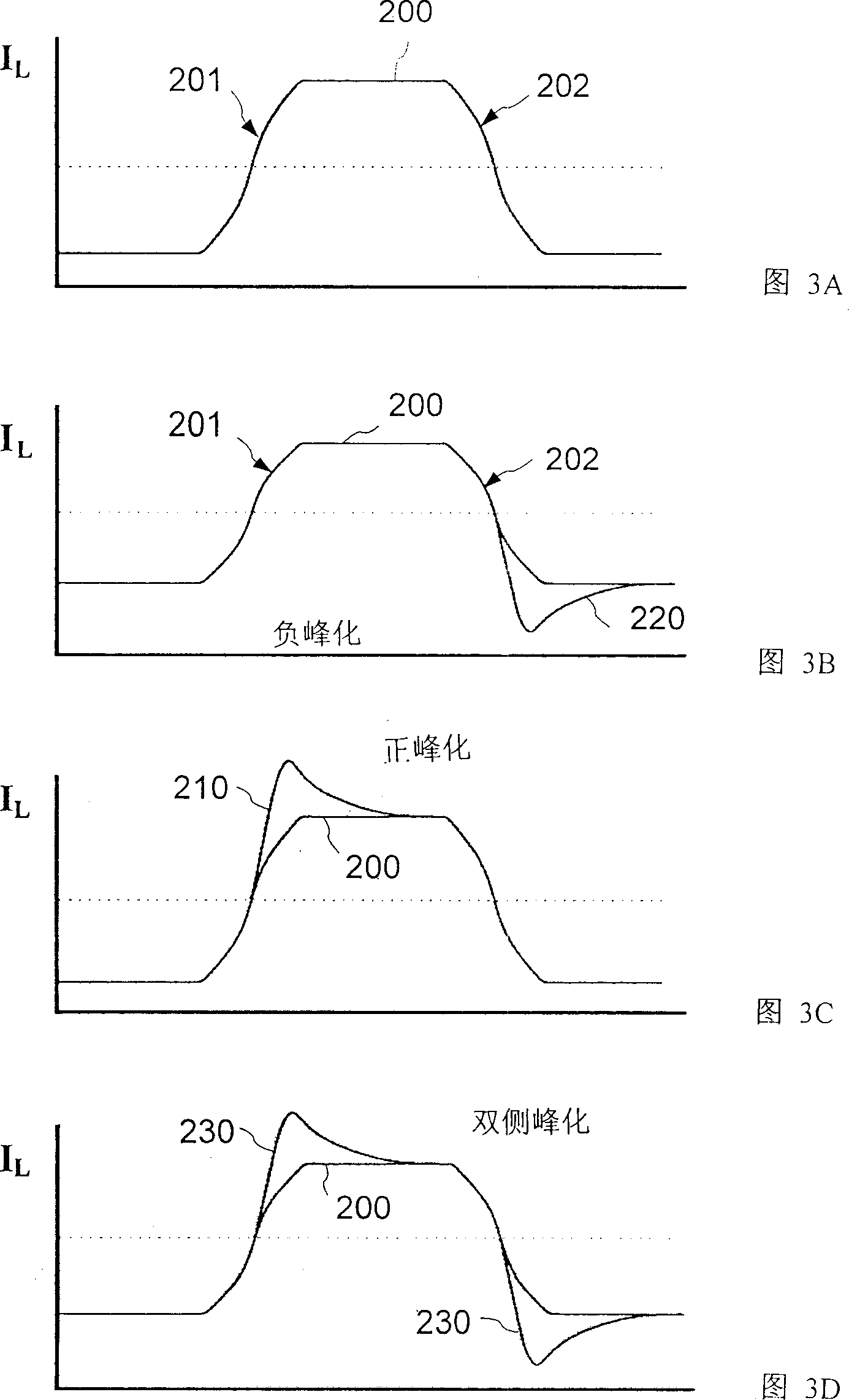
[0010] [10] Among other disadvantages, many existing pulse shaping circuits cannot distinguish between the rising and falling edges of the driving electrical pulse; that is, the peaking pulse applied to the rising edge by the circuit is also applied to the falling edge of the driving pulse with the same amplitude
However, some types of optical transmitters, namely many types of semiconductor lasers, require a larger peaking pulse on the rising edge of the drive current pulse than on the falling edge of the drive current pulse, because lasers generally require more on-pulses than off-pulses. big open pulse

Method used


Image

  • Pulse shaping circuit
  • Pulse shaping circuit
  • Pulse shaping circuit

Examples


Embodiment Construction

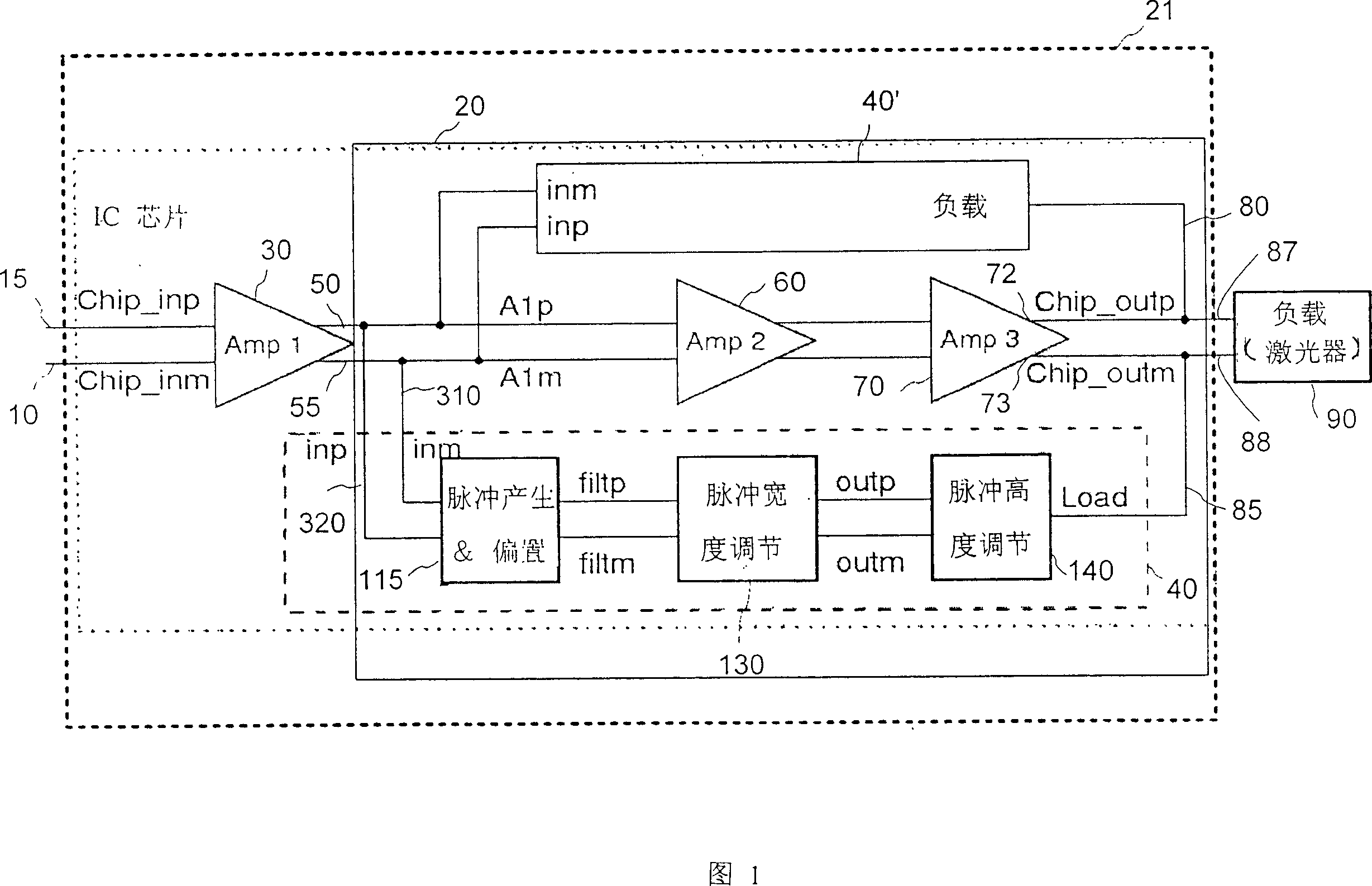
[0028] [28] Here, the present invention may be described in terms of various functional components. It should be understood that such functional elements may be realized by any number of hardware or structural elements configured to perform the specified functions. For example, the present invention may utilize various integrated components consisting of different electrical devices such as resistors, transistors, capacitors, diodes, etc., whose values ​​may be suitably configured for different intended purposes. In addition, it should be noted that in the schematic circuits, when different components can be suitably coupled or connected to other components, this connection and coupling can be achieved through direct connections between components, or through other components and connected to the device. Also, redundant details have not been included in order to facilitate explanation and understanding of the present invention.

[0029] [29] An exemplary embodiment of a puls...


PUM


Abstract

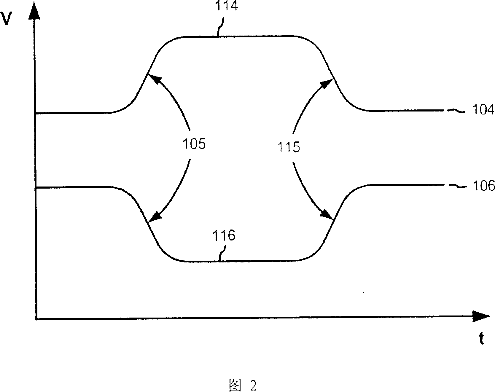
The invention relates to a pulse shaping circuit for shaping electrical pulses driving an optical transmitter, e.g. a lased diode or an LED, and for providing electrical pulses having independently height and width-adjustable peaking at the edges thereof. The pulse shaping circuit of the present invention includes a high-pass RC filter with a differential output for providing transient electrical pulses from an input differential pulse, an adjustable voltage offset generating circuit, a differential amplifier for adjusting the width of the transient electrical pulses in dependence on the adjustable voltage offset, and a variable-gain current-steering amplifier for producing transient pulses with independently adjustable width and height.

Description

technical field [0001] [1] The present invention relates to a pulse shaping circuit, and in particular to a circuit for adding peaking with adjustable width and height to pulse edges. Background technique [0002] [2] In many applications, a light emitter such as a laser diode (LD) or light emitting diode (LED) is driven by a pulsed current to alternately turn on or off the light source and generate light pulses. [0003] [3] In general, it is desirable for the light pulse to have a roughly rectangular shape and to follow the current pulse as closely as possible. However, there is a time delay associated with switching on or off the light emitter, eg between a switching transition of the drive current of the emitter and an associated switching transition of the light output of the emitter. Similarly, there is a time delay between the on-off transition of the drive current of the emitter and the associated off-on transition of the light output of the emitter. This time dela...

Claims


Application Information

Patent Timeline
Patent Type & Authority Applications(China)
IPC IPC(8): H04B10/04
CPCH03K5/06H03K5/12H01S5/042
Inventor 斯蒂芬·J.·鲍姆加特纳布拉德·安东尼·纳兹克
Owner LUMENTUM OPERATIONS LLC
Learn More