

Two-dimensional photonic crystal with large absolute band gap
A two-dimensional photonic crystal and square lattice technology, which is applied in crystal growth, laser, single crystal growth, etc., can solve the problems of small choice, difficult application, and difficult preparation
- Summary
- Abstract
- Description
- Claims
- Application Information
AI Technical Summary
Problems solved by technology
Method used
Image

Examples
Embodiment Construction
[0015] The preferred embodiments of the present invention will be described in detail below in conjunction with the accompanying drawings.
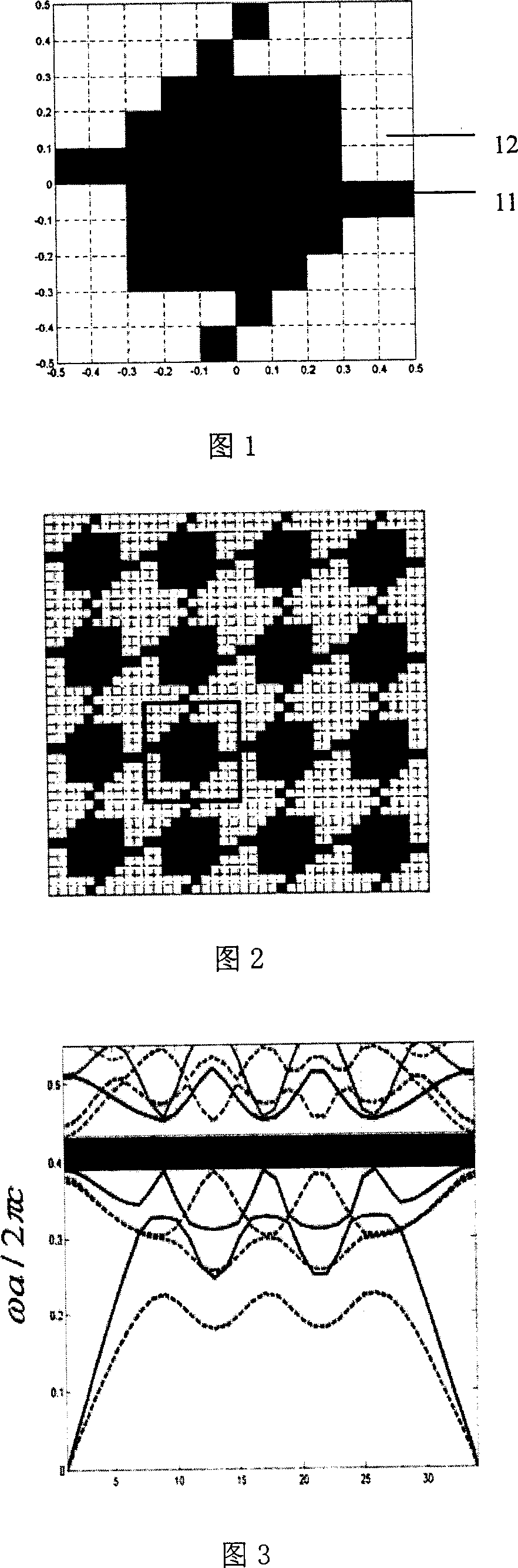
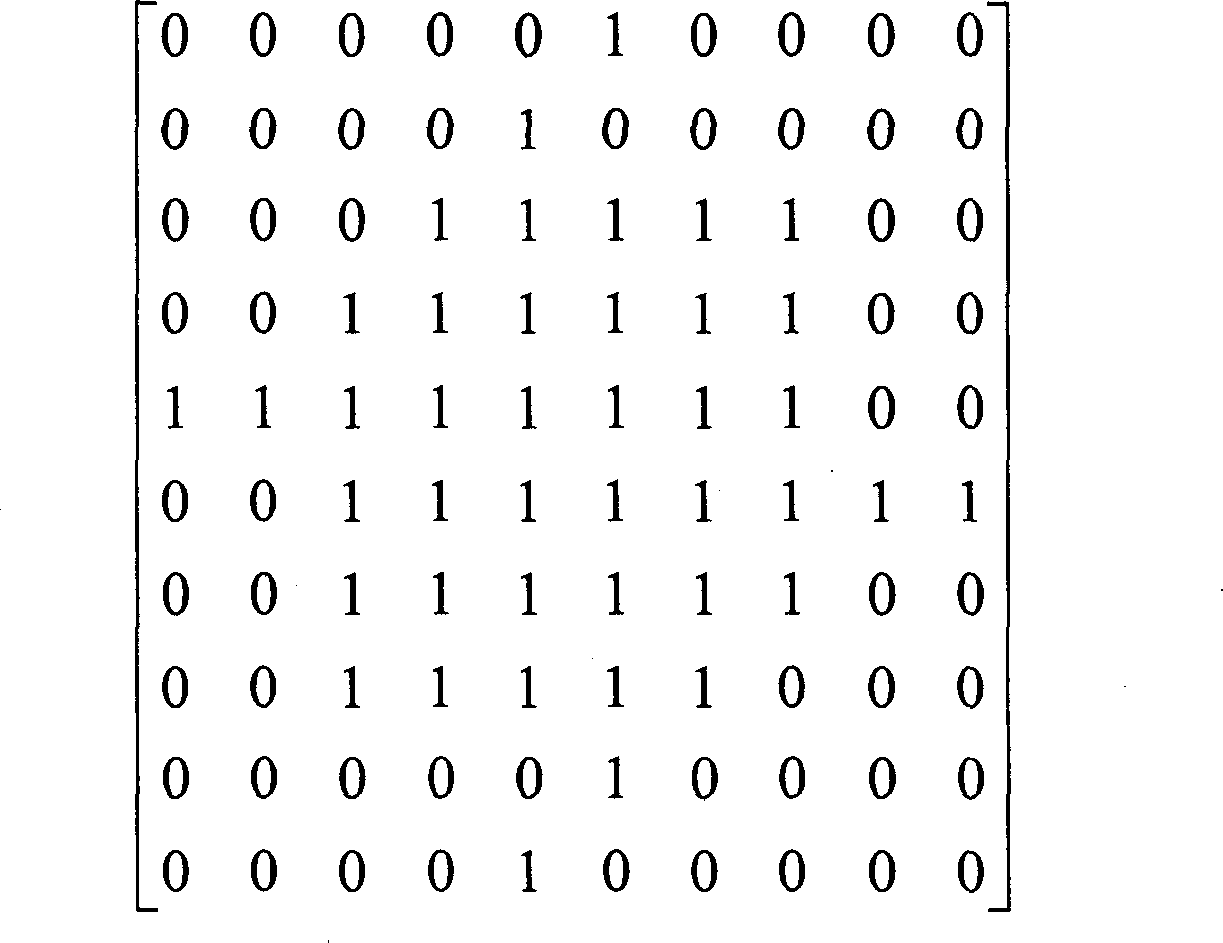
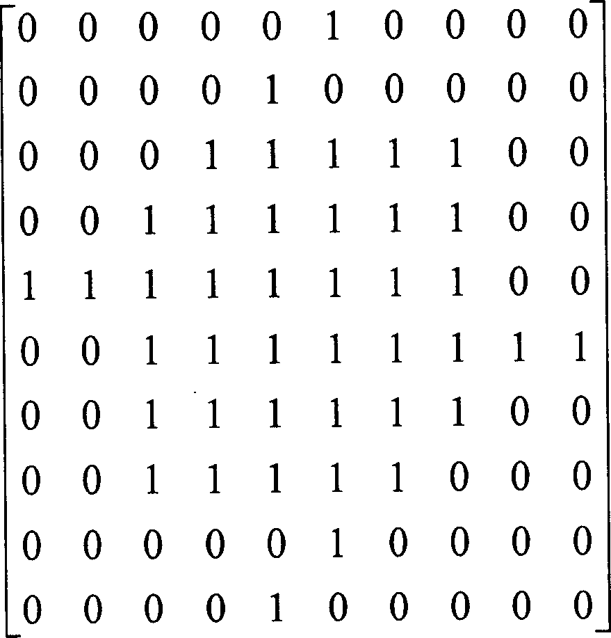
[0016] As shown in FIG. 1 , the original cell of the two-dimensional photonic crystal, the original cell of the two-dimensional photonic crystal of the present invention is composed of 10×10 square pixels. The black portion 11 represents a high refractive index material, and the white portion 12 represents a low refractive index material. The high refractive index part is made of silicon with a dielectric constant of 11.56; the low refractive index part is made of air with a dielectric constant of 1. The lattice constant a is taken as 1 μm, the pixel, that is, the side length of the square pillar is 100 nm, and the size of the square pillar is 100 nm×100 nm. This structure verifies the rule summed up by people: large absolute bandgap is more likely to appear in the photonic crystal structure in which the distribution of high dielectric m...
PUM
 Abstract
Description
Claims
Application Information