Current limited bilateral MOSFET switch with reduced switch resistance and lower manufacturing cost
一种电流限制、P-FET的技术,应用在提供电流限制双向MOSFET开关的制造,经改进的电路结构设计领域,能够解决高功率消耗、低工作效率等问题
- Summary
- Abstract
- Description
- Claims
- Application Information
AI Technical Summary
Problems solved by technology
Method used
Image
Examples
Embodiment Construction
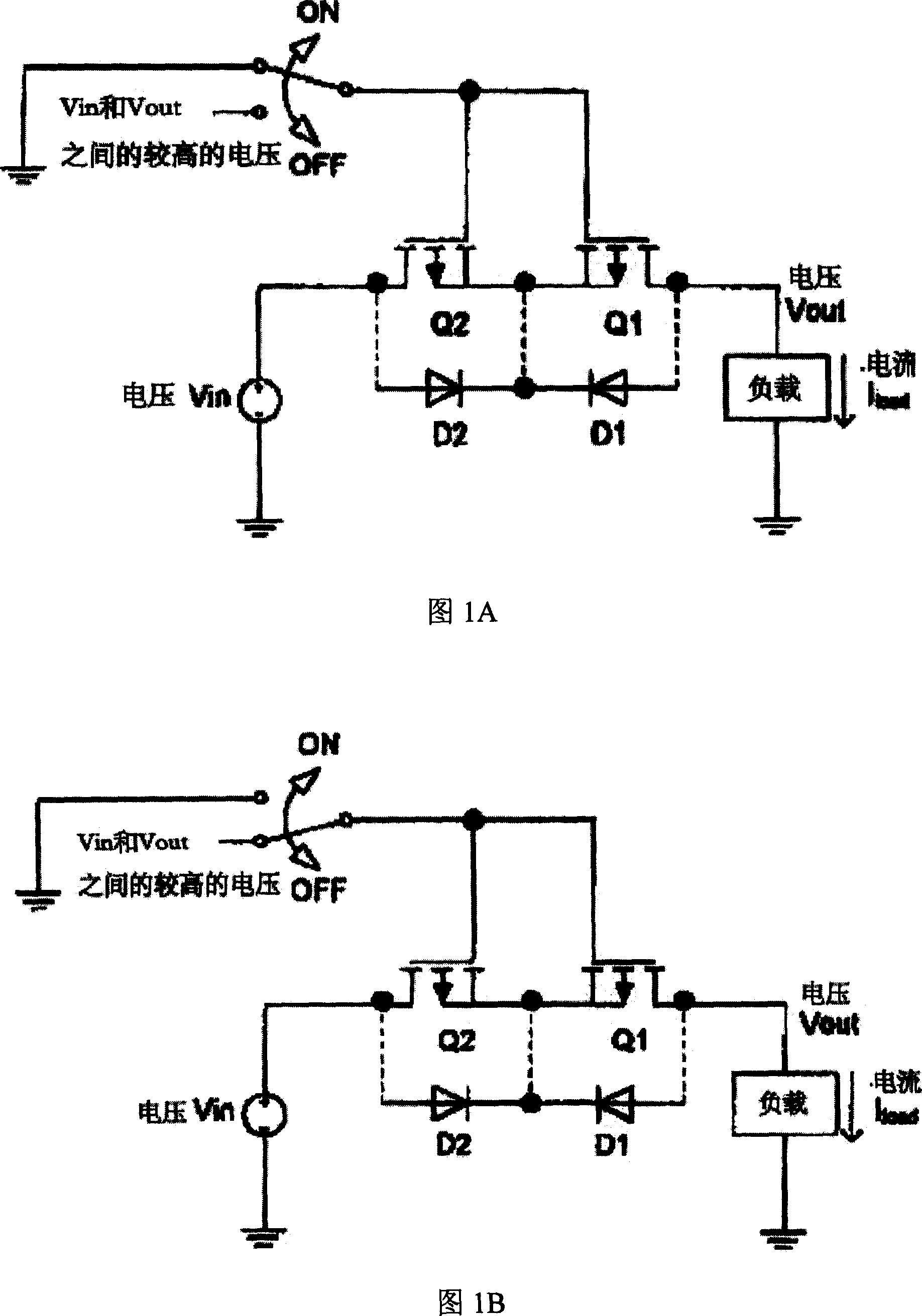
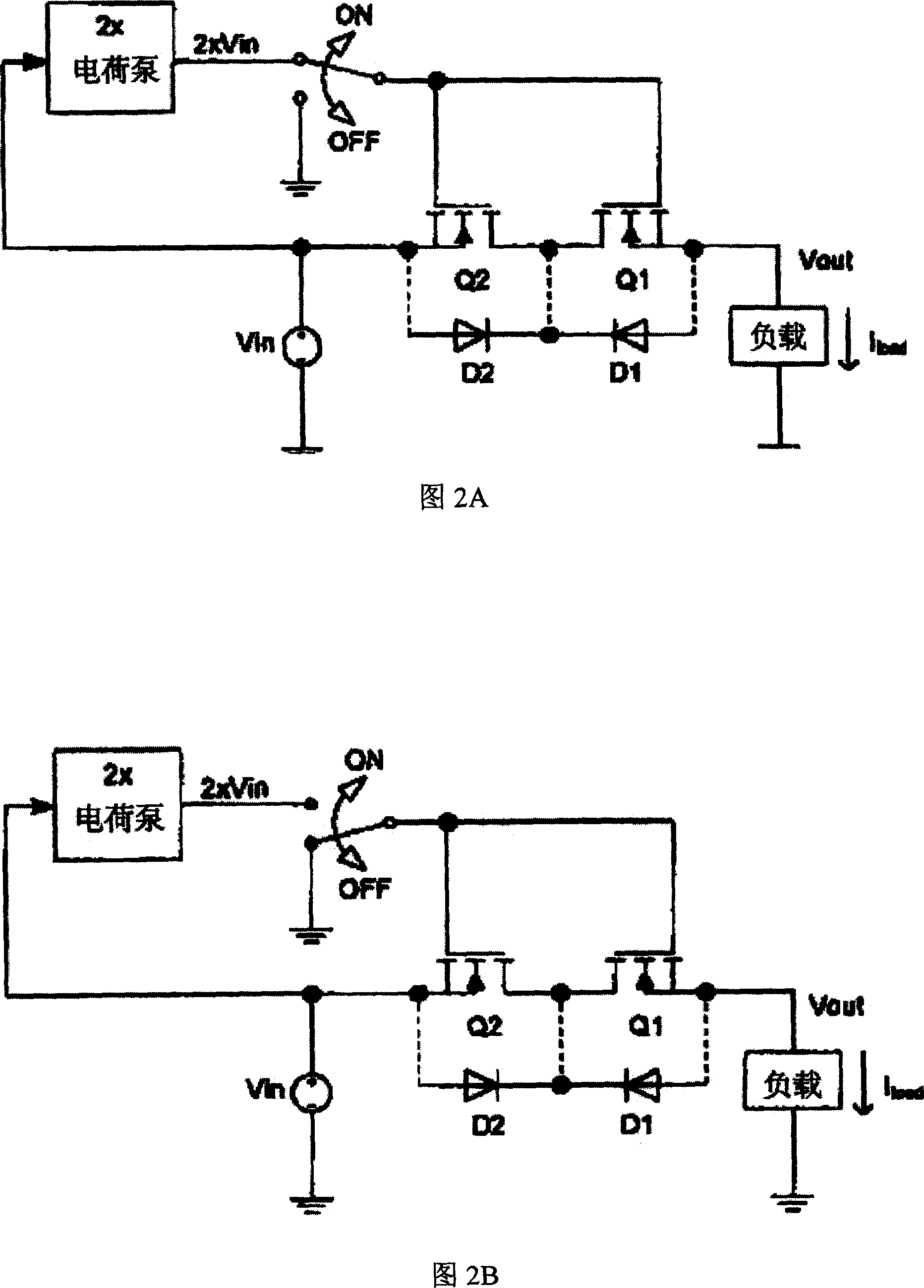
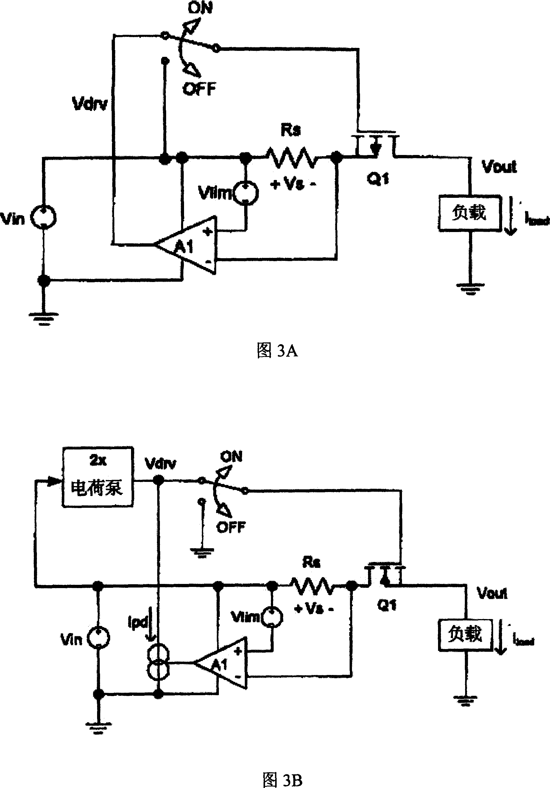
[0021] Refer to FIG. 5A for a circuit diagram of a novel and improved current-limited bidirectional switch implemented with two common-source P-FET transistors to overcome the technical difficulties described above. The current limiting bidirectional power switch 100 includes two common source P-FET transistors 110 and 120 shown as Q1 and Q2 respectively, with a common source node 125 shown. The second P-FET bidirectional function transistor 120 has the function of a sense resistor, Rs shown in FIG. 4A . The voltage drop across P-FET transistor 120 is sensed by amplifier 130 shown as Al. The voltage drop across the P-FET transistor 120 is represented by the value of Iload×Rdson2, where Iload is the current flowing through the load 140 and Rdon2 is the resistance between the source and drain of the second P-FET transistor 120 . The voltage drop across the P-FET transistor 120 is compared to the current limit voltage Vlim150 implemented to prevent the current from exceeding the...
PUM
 Abstract
Description
Claims
Application Information
 - R&D Engineer
- R&D Manager
- IP Professional
- Industry Leading Data Capabilities
- Powerful AI technology
- Patent DNA Extraction
Browse by: Latest US Patents, China's latest patents, Technical Efficacy Thesaurus, Application Domain, Technology Topic, Popular Technical Reports.
© 2024 PatSnap. All rights reserved.Legal|Privacy policy|Modern Slavery Act Transparency Statement|Sitemap|About US| Contact US: help@patsnap.com


