Capacitance structure for the integrated circuit

A technology of integrated circuits and capacitor structures, applied in circuits, electrical components, electric solid-state devices, etc., can solve problems such as reducing the efficiency of integrated circuits and mismatching MIM capacitor components

Active Publication Date: 2007-07-11
VIA TECH INC
View PDF0 Cites 3 Cited by
  • Summary
  • Abstract
  • Description
  • Claims
  • Application Information

AI Technical Summary

Problems solved by technology

As a result, the metal lines 103 and 105 embedded in the uneven dielectric layer 102 will make the mismatch between the MIM capacitor elements more serious, reducing the performance of the integrated circuit

Method used


Image

  • Capacitance structure for the integrated circuit
  • Capacitance structure for the integrated circuit
  • Capacitance structure for the integrated circuit

Examples


Embodiment Construction

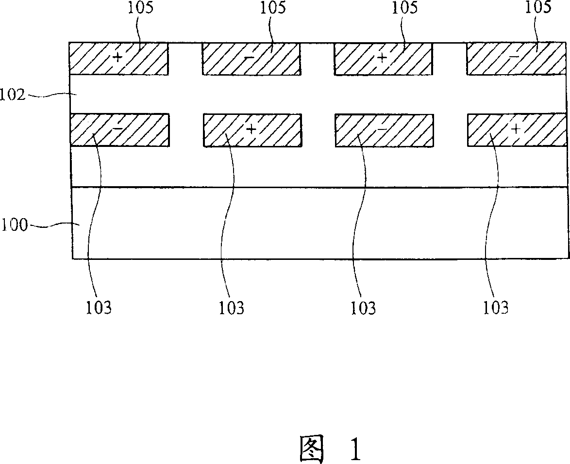
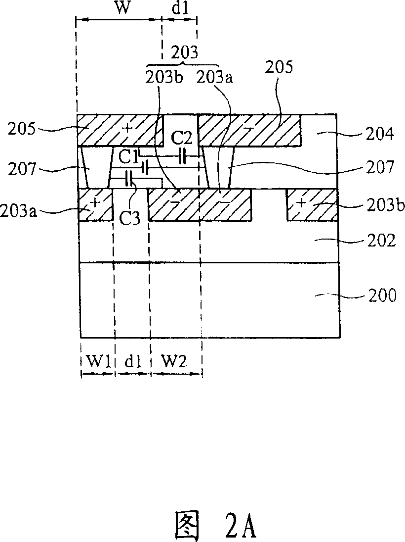
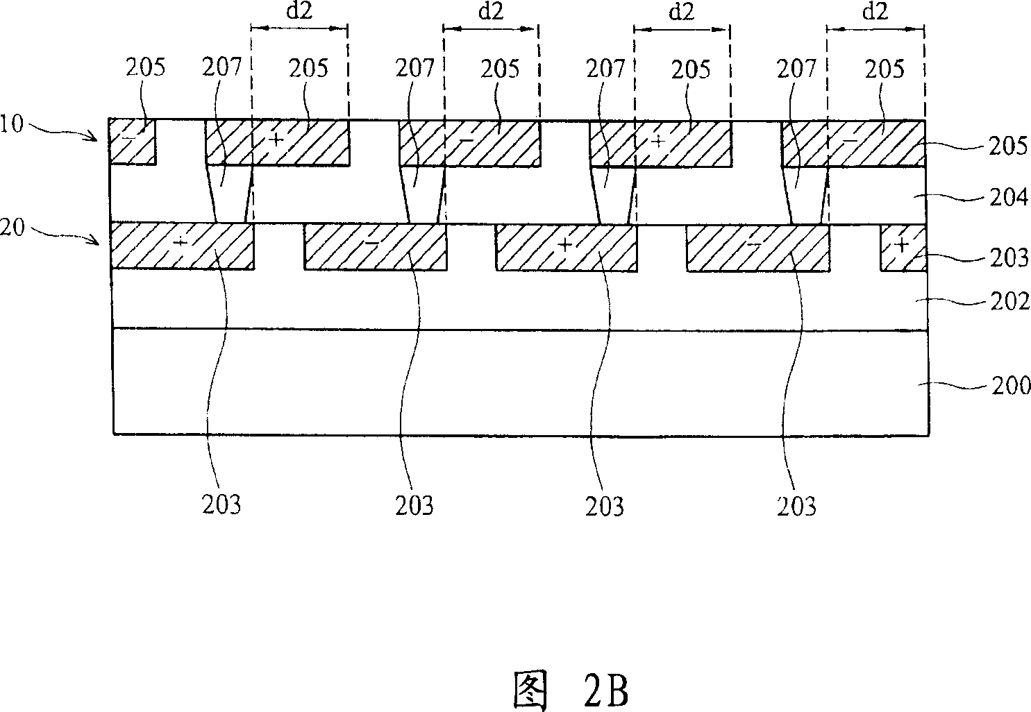
[0024] The present invention relates to an improved capacitor structure suitable for different integrated circuit designs, such as mixed signal circuits, radio frequency circuits, and analog circuits. 2A and 2B illustrate the embodiment of the present invention for the capacitor structure of the integrated circuit, wherein FIG. 2A shows a schematic cross-sectional schematic diagram of two parallel (side by side) capacitor structure unit according to the embodiment of the present invention, and FIG. 2B draws A cross-sectional schematic diagram of a multiple capacitor structure composed of capacitor structural units in FIG. 2A is shown. Referring to FIG. 2A , the capacitor structure unit includes a dielectric layer and wires 203 and 205 embedded therein. The dielectric layer can be an intermetal dielectric (IMD) layer disposed on a substrate 200 . The substrate 200 can be a silicon substrate or other semiconductor substrates, which can include various elements, such as transist...


PUM


Abstract

This invention discloses one integration circuit capacitor structure, which comprises one dielectric layer and first, second and third wires, wherein, the dielectric layer is set on one underlay; first wire is imbedded into first level of dielectric layer; the second and third wires are imbedded into second level lower than first level with certain distance; the second wire is covered by one projection on underlay and the third wire is covered by one projection on underlay.

Description

technical field [0001] The present invention relates to a capacitor structure for integrated circuits, and more particularly to a lateral capacitor structure that can improve capacitance mismatch. Background technique [0002] Many digital and analog components and circuits have been successfully used in semiconductor integrated circuits. The above components include passive components such as resistors, capacitors or inductors. A typical semiconductor integrated circuit includes a silicon substrate. More than one dielectric layer is disposed on the substrate, and more than one metal layer is disposed in the dielectric layer. These metal layers can be used to form on-chip components, such as on-chip metal-insulator-metal (MIM) capacitors, through current semiconductor process technology. [0003] A typical metal-insulator-metal (MIM) capacitor element includes two conductive plates, one of which is above the other and parallel to each other, and a layer of dielectric mate...

Claims


Application Information

Patent Timeline
Patent Type & Authority Applications(China)
IPC IPC(8): H01L27/02H01L23/522
Inventor 陈骏盛曾英哲
Owner VIA TECH INC
Why Eureka
Try Eureka