Eureka AIR delivers breakthrough ideas for toughest innovation challenges, trusted by R&D personnel around the world.

Lithographic apparatus, device manufacturing method and associated data processing apparatus and computer program product

a technology of data processing apparatus and lithographic apparatus, which is applied in the direction of microlithography exposure apparatus, instruments, photomechanical treatment, etc., can solve the problems of uneconomical correctability in practice, uncorrectable noise, and overlay error, and achieve the effect of improving overlay performance and adversely affecting throughpu

Active Publication Date: 2018-07-17
ASML NETHERLANDS BV
View PDF28 Cites 3 Cited by
  • Summary
  • Abstract
  • Description
  • Claims
  • Application Information

AI Technical Summary

Benefits of technology

[0009]It is desirable to improve overlay performance without adding to the space occupied by alignment marks required on each substrate, and without adversely impacting throughput. It is further desirable that such improvement be obtained if possible using existing lithographic apparatus and associated hardware.

Problems solved by technology

A key performance parameter of the lithographic process is the overlay error.
This error, often referred to simply as “overlay” is the error in placing a product features it the correct position relative to features formed in previous layers.
Some of these errors may be uncorrectable noise, for example, but others are correctable using available techniques in theory, but not economically correctable in practice.
To increase the spatial density and / or measurement frequency of alignment marks and overlay targets would adversely affect both throughput of the lithographic process (wafers per hour) and the functional device area available on each substrate.

Method used


Image

  • Lithographic apparatus, device manufacturing method and associated data processing apparatus and computer program product
  • Lithographic apparatus, device manufacturing method and associated data processing apparatus and computer program product
  • Lithographic apparatus, device manufacturing method and associated data processing apparatus and computer program product

Examples


Embodiment Construction

[0035]Before describing embodiments of the invention in detail, it is instructive to present an example environment in which embodiments of the present invention may be implemented.

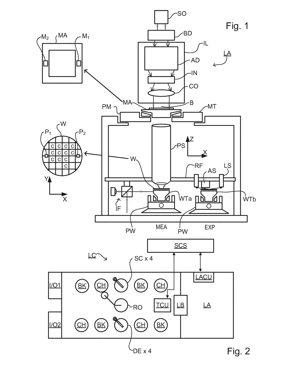
[0036]FIG. 1 schematically depicts a lithographic apparatus LA. The apparatus includes an illumination system (illuminator) IL configured to condition a radiation beam B (e.g., UV radiation or DUV radiation), a patterning device support or support structure (e.g., a mask table) MT constructed to support a patterning device (e.g., a mask) MA and connected to a first positioner PM configured to accurately position the patterning device in accordance with certain parameters; a substrate table (e.g., a wafer table) WT constructed to hold a substrate (e.g., a resist coated wafer) W and connected to a second positioner PW configured to accurately position the substrate in accordance with certain parameters; and a projection system (e.g., a refractive projection lens system) PS configured to project a pattern im...


PUM

PropertyMeasurementUnit
heightaaaaaaaaaa
widthaaaaaaaaaa
wavelengthaaaaaaaaaa

Abstract

A lithographic apparatus applies a pattern repeatedly to target portions across a substrate. Prior to applying the pattern an alignment sensor measures positions of marks in the plane of the substrate and a level sensor measures height deviations in a direction normal to the plane of the substrate. The apparatus applies the pattern to the substrate while positioning the applied pattern using the positions measured by the alignment sensor and using the height deviations measured by the level sensor. The apparatus is further arranged to calculate and apply corrections in the positioning of the applied pattern, based on derivatives of the measured height deviations. The corrections may be calculated on an intrafield and / or interfield basis. The corrections may be based on changes between the observed height deviations and height deviations measured previously on the same substrate.

Description

BACKGROUND[0001]Field of the Invention[0002]This application is the U.S. national phase entry of PCT patent application no, PCT / EP2014 / 072717, which was filed on Oct. 23, 2014, which claims the benefit of EP patent application no. 14150722.8, which was filed on Jan. 10, 2014, and which is incorporated herein in its entirety by reference.[0003]The present invention relates to a method for determining overlay errors in a lithographic apparatus. The present invention further relates to methods of manufacturing devices using lithographic apparatus calibrated by such a method, and to data processing apparatuses and computer program products for implementing parts of such a method[0004]Background Art[0005]A lithographic apparatus is a machine that applies a desired pattern onto a substrate, usually onto a target portion of the substrate. A lithographic apparatus can be used, for example, in the manufacture of integrated circuits (ICs). In that instance, a patterning device, which is alter...

Claims


Application Information

Patent Timeline
Patent Type & Authority Patents(United States)
IPC IPC(8): G03F7/20G03F9/00
CPCG03F7/70141G03F9/7092G03F9/7003G03F7/70508G03F7/706G03F7/70766G03F7/70775
Inventor CEKLI, HAKKI ERGUNLIU, XING LANSLOTBOOM, DAAN MAURITSTEL, WIM TJIBBOVAN DER SANDEN, STEFAN CORNELIS THEODORUSVAN HAREN, RICHARD JOHANNES FRANCISCUS
Owner ASML NETHERLANDS BV
Why Eureka
Eureka Blog
Learn More