Organic EL display device

a display device and organic technology, applied in the direction of thermoelectric device junction materials, semiconductor devices, electrical apparatus, etc., can solve the problem that the plurality of electrically separated films cannot be formed by merely irradiating lasers, and achieve the effect of reducing manufacturing costs, reducing manufacturing processes, and reducing manufacturing costs

Active Publication Date: 2018-07-17
JAPAN DISPLAY INC
View PDF15 Cites 0 Cited by
  • Summary
  • Abstract
  • Description
  • Claims
  • Application Information

AI Technical Summary

Benefits of technology

[0006]Since different signals are respectively provided to the electrodes included in the pixels, the films to which the different signals are provided need to be electrically separated. Further, in order to reduce the manufacturing cost, it is preferable to reduce the number of manufacturing processes. Therefore if a plurality of electrically separated films can be formed in a single film formation process, the manufacturing cost can be reduced.
[0012]However, according to this configuration, an area of a rib opening part 326 becomes small due to the rib 324, and the light emitting area per one pixel 208 becomes small. Thus, the display quality deteriorates due to this configuration. Further, if a large current is supplied to the organic EL film 328 so as to compensate the decrease in the light emitting area, the life span of the organic EL film 328 becomes shorter.
[0013]The present invention has been made in view of the above problems, and the object thereof is to provide an organic EL display device, which is manufactured in a small number of manufacturing processes, and has a high display quality and a long life span.

Problems solved by technology

However, a plurality of electrically separated films cannot be formed by merely irradiating laser.

Method used


Image

  • Organic EL display device
  • Organic EL display device
  • Organic EL display device

Examples


Embodiment Construction

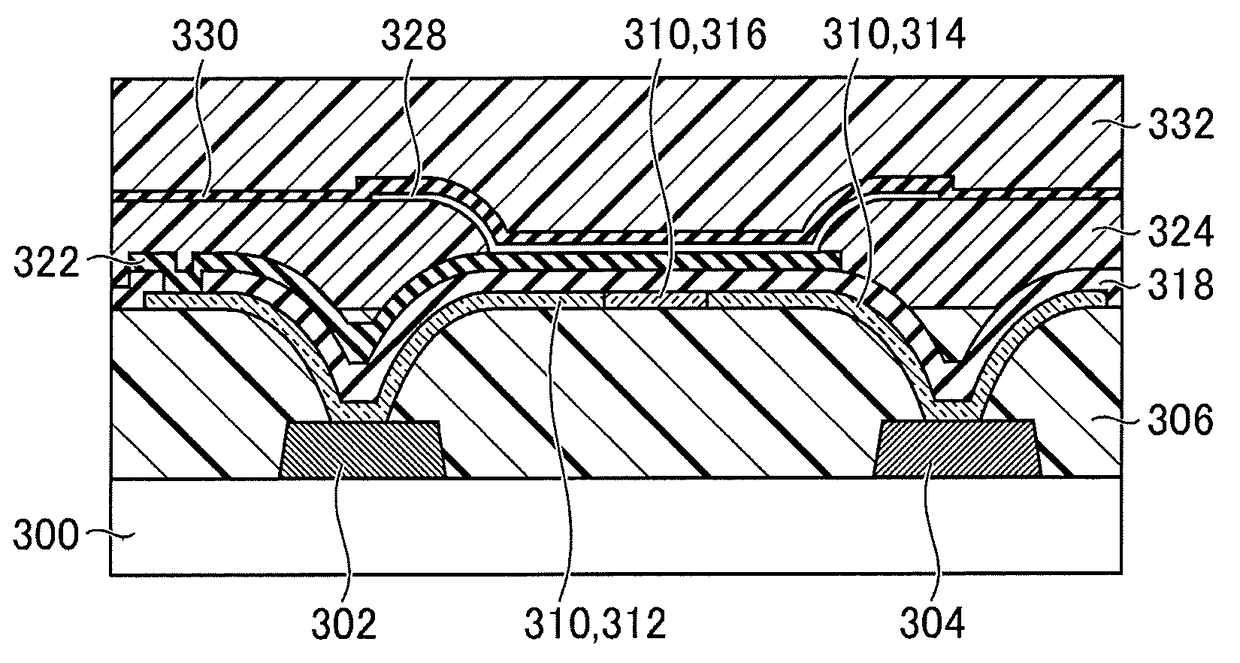
[0033]Below, respective embodiments of the present invention are explained with reference to the accompanying drawings. Note that disclosed embodiments are merely examples, and an appropriate variation that a person skilled in the art can easily arrive at without departing from the spirit of the present invention is naturally included in the scope of the present invention. Further, while the width, thickness, shape, and the like of each part in the drawings may be illustrated schematically as compared with actual embodiments in order to clarify the explanation, these are merely examples and an interpretation of the present invention should not be limited thereto. Furthermore, in the specification and respective drawings, the same reference symbols may be applied to elements similar to those that have already been illustrated in another drawing and a detailed explanation of such elements may be omitted as appropriate.

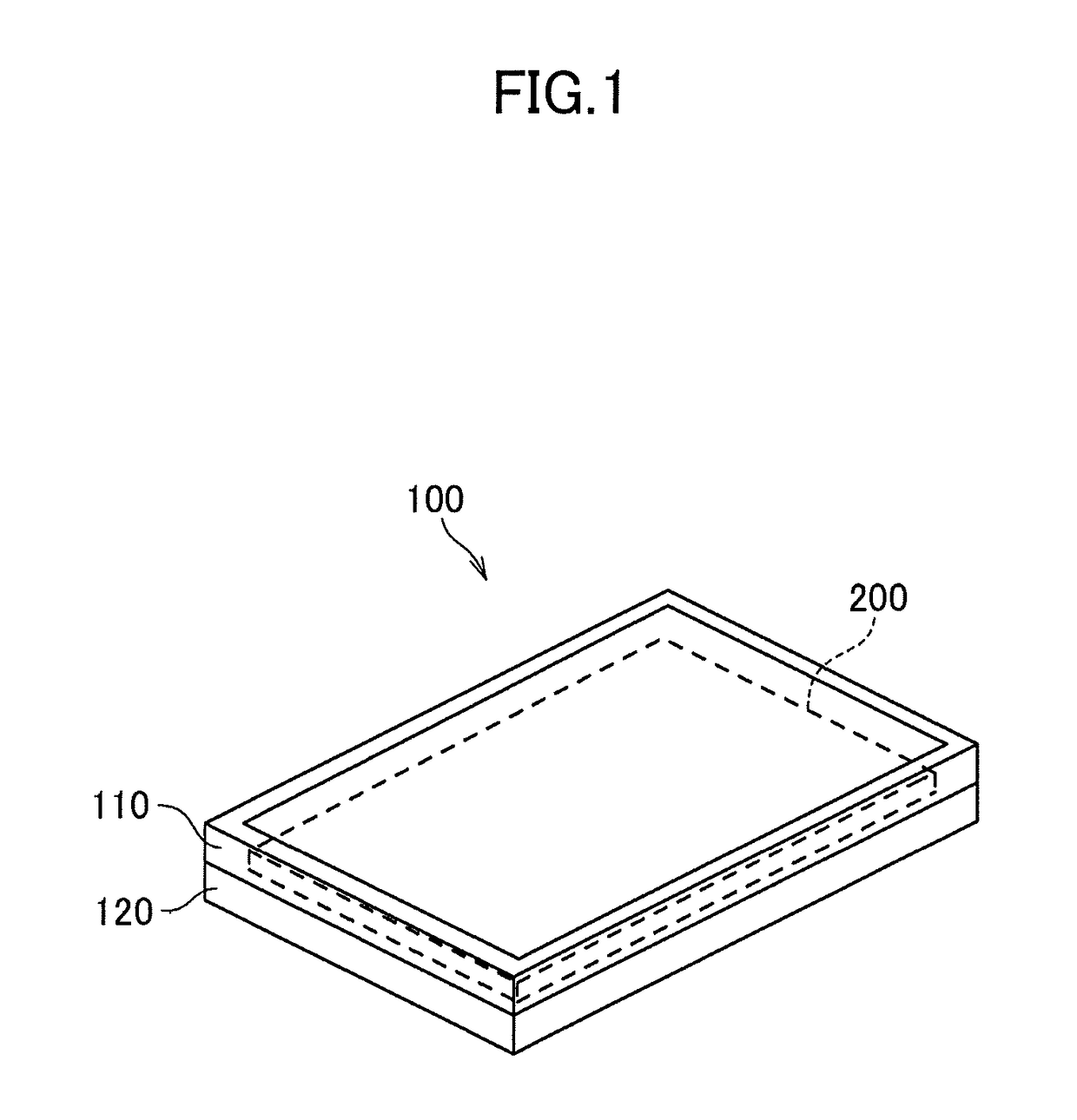
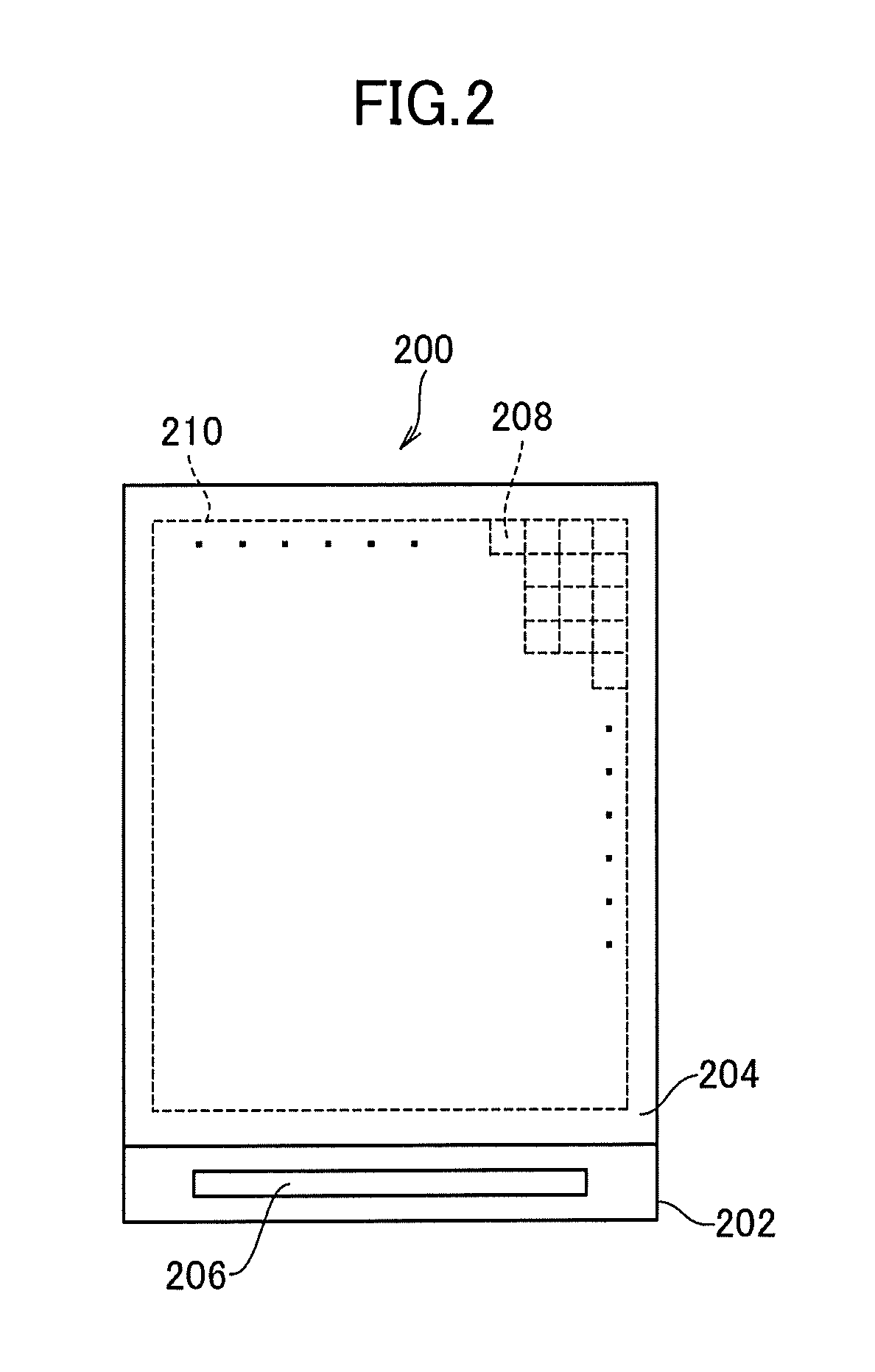
[0034]FIG. 1 is a diagram that schematically illustrates an organic...


PUM


Abstract

An organic EL display device includes a substrate on which a plurality of driver transistors are formed, a first wiring that supplies an electric voltage in accordance with a display image via one of the driver transistors, an organic EL film that emits light, an anode electrode, and an auxiliary electrode film including a first low resistance part, a second low resistance part separated from the first low resistance part, and a high resistance part disposed between the first low resistance part and the second low resistance part. The first low resistance part is electrically connected to the first wiring and the anode electrode. The second low resistance part forms an electrostatic capacitance between the anode electrode and itself. The high resistance part has an electric resistance higher than those of the first low resistance part and the second low resistance part.

Description

CROSS-REFERENCE TO RELATED APPLICATION[0001]The present application claims priority from the Japanese Application JP2016-199034 filed on Oct. 7, 2016, the content of which is hereby incorporated by reference into this application.BACKGROUND OF THE INVENTION1. Field of the Invention[0002]One or more embodiments of the present invention relate to an organic EL display device.2. Description of the Related Art[0003]Recent years, research and development of quality enhancement and manufacturing cost reduction of an organic EL display device is proceeded. An organic EL display device displays an image by a plurality of pixels in which an electric circuit is formed. Since the electric circuit includes a plurality of electrodes, capacitors and the like to which signals are supplied, for the quality enhancement and the manufacturing cost reduction as above, technological development for a film constituting electrodes and capacitors is important.[0004]For example, Japanese Patent Application ...

Claims


Application Information

Patent Timeline
Patent Type & Authority Patents(United States)
IPC IPC(8): H01L29/08H01L35/24H01L51/52H01L27/32
CPCH01L51/5212H01L27/3262H01L51/5209H01L27/3276H01L27/3265H10K59/1216H10K59/1315H10K59/80516H10K59/80515H10K50/814H10K50/813H10K59/131H10K59/1213
Inventor TOKUDA, NAOKI
Owner JAPAN DISPLAY INC
Why Eureka
Try Eureka