

Wafer level integrated circuit probe array and method of construction
a probe array and integrated circuit technology, applied in the field of integrated circuit fabrication and testing, can solve the problems that the testing of ic-packed lead will not work without substantial modification, and achieve the effect of easy machine-aware sidewalls
- Summary
- Abstract
- Description
- Claims
- Application Information
AI Technical Summary
Benefits of technology
Problems solved by technology
Method used
Image

Examples
Embodiment Construction
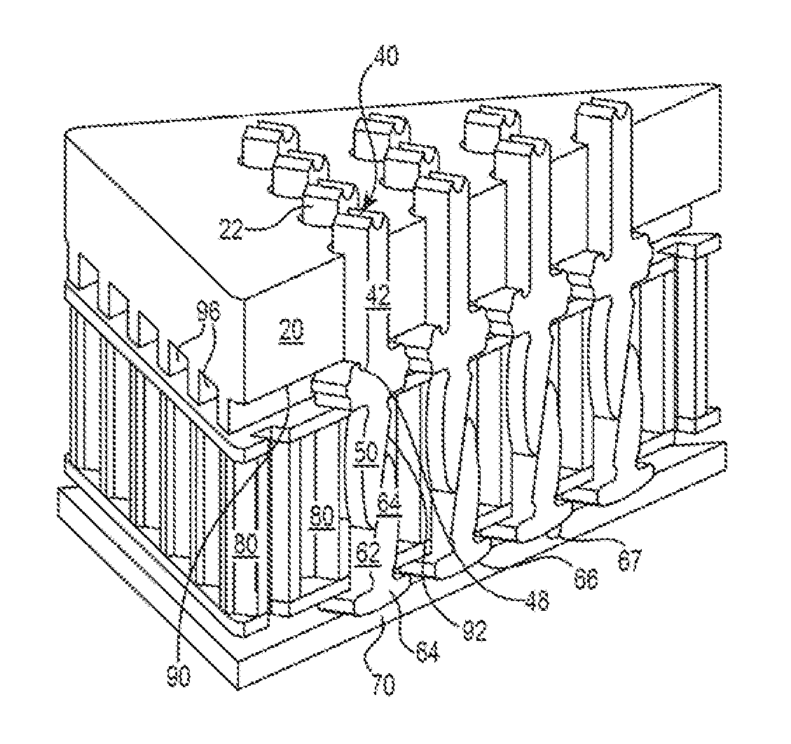
[0139]A typical IC wafer contains between 1 k-22 k dies typically organized in a regular matrix separated by horizontal and vertical scribe lines, for later cutting into individual dies or chips to be mounted in an IC enclosure with leads or contacts. This disclosure is primarily directed to testing of an individual dies or groups of dies in an array such as a pattern of generally geographically adjacent dies, or multiple arrays simultaneously, before they are cut along the scribe lines, whereafter, each die is inserted into an IC package with leads or contacts.
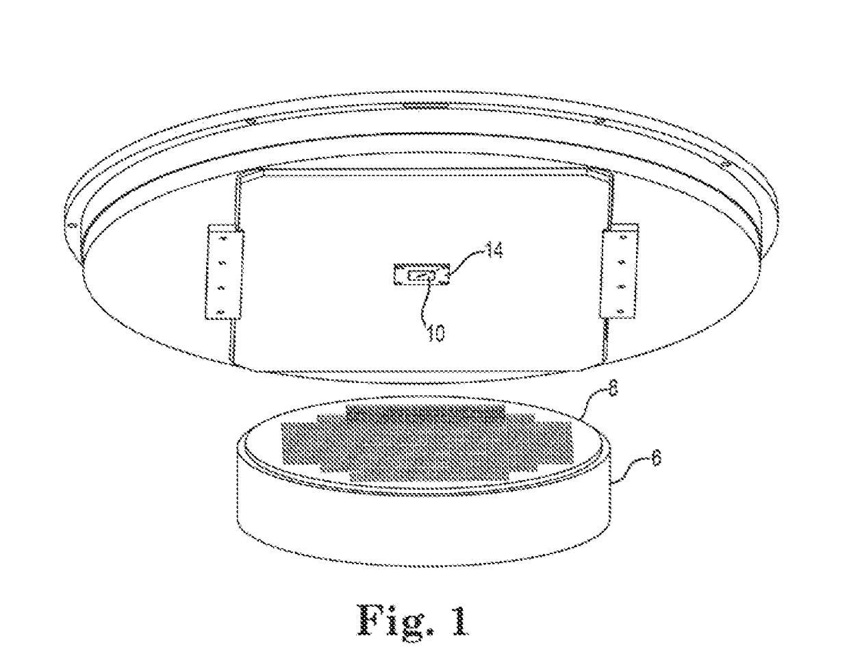
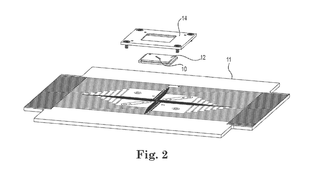
[0140]In the preferred embodiment, as shown in FIGS. 1 and 2, a probe array of contacts 10 is held, preferably close press fit registration to prevent movement, into a pin guide plate / pin guide 12 which itself is affixed onto probe retainer 14 by means of a retainer. Said retainer may include a picture frame opening which has a stepped ledge to accommodate a like ledge on the pin guide plate 12. It is preferable to restrict f...
PUM
 Abstract
Description
Claims
Application Information