
Method for producing nanocrystals with controlled dimensions and density

a nanocrystal and density control technology, applied in the direction of semiconductor/solid-state device manufacturing, basic electric elements, electric devices, etc., can solve the problems of reducing the thickness of the thin layer of semiconductor, unable to achieve large homogeneous surfaces in terms of thickness, and not being able to obtain particles of small dimensions

Active Publication Date: 2018-10-23
COMMISSARIAT A LENERGIE ATOMIQUE ET AUX ENERGIES ALTERNATIVES
View PDF12 Cites 0 Cited by
  • Summary
  • Abstract
  • Description
  • Claims
  • Application Information

AI Technical Summary

Benefits of technology

[0009]There thus exists a need to propose a method for producing nanocrystals of semiconductor making it possible to reduce the dimensions of the nanocrystals and to increase the surface density with which the nanocrystals are distributed, which is notably compatible with obtaining nanocrystals of dimensions for example less than around 50 nm, without having to implement thinning of the thin layer of semiconductor to dewet to obtain a thickness that depends on the desired dimensions for the nanocrystals, add carbon species to the thin layer of semiconductor or induce a stress in the thin layer of semiconductor.
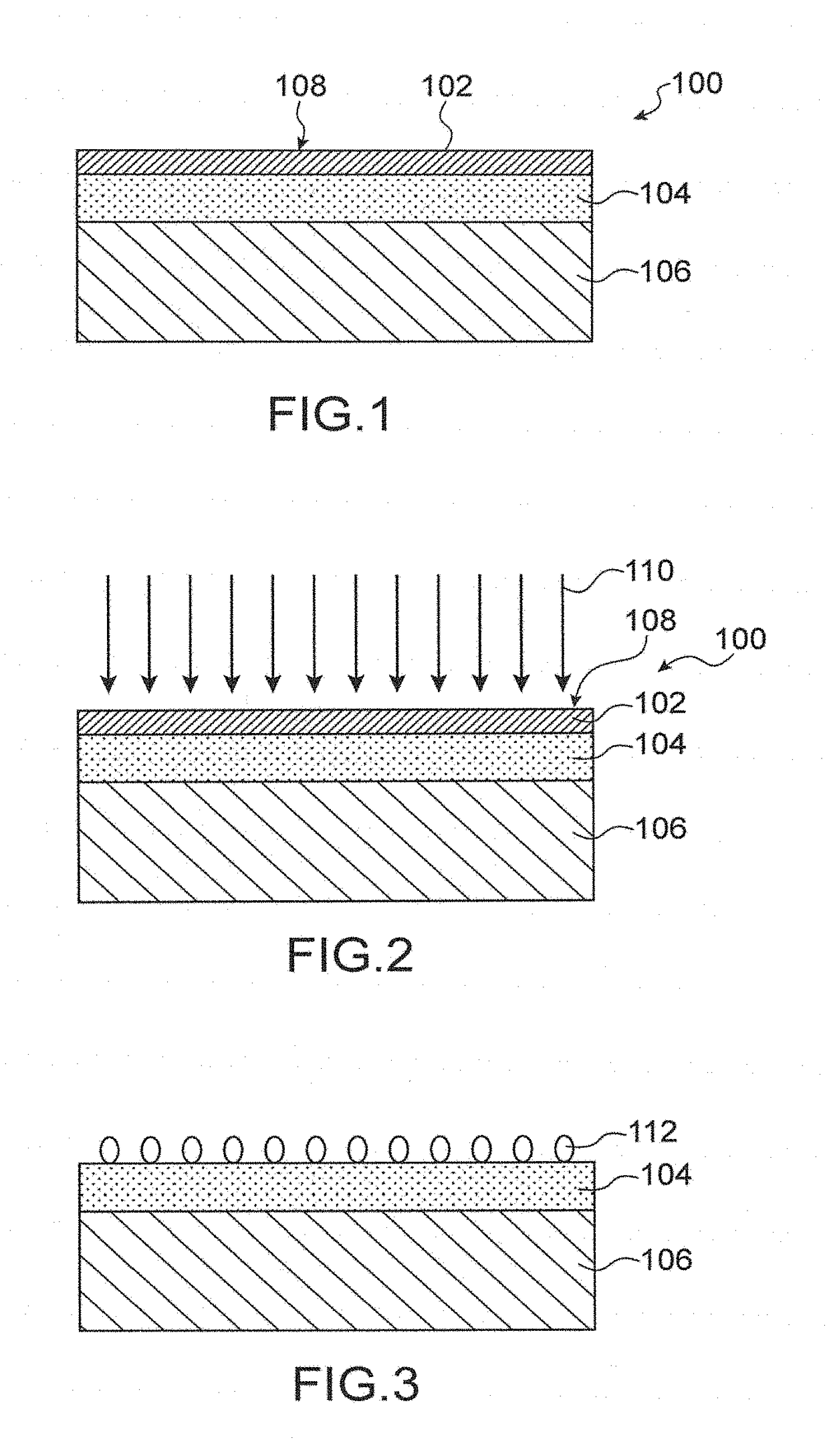
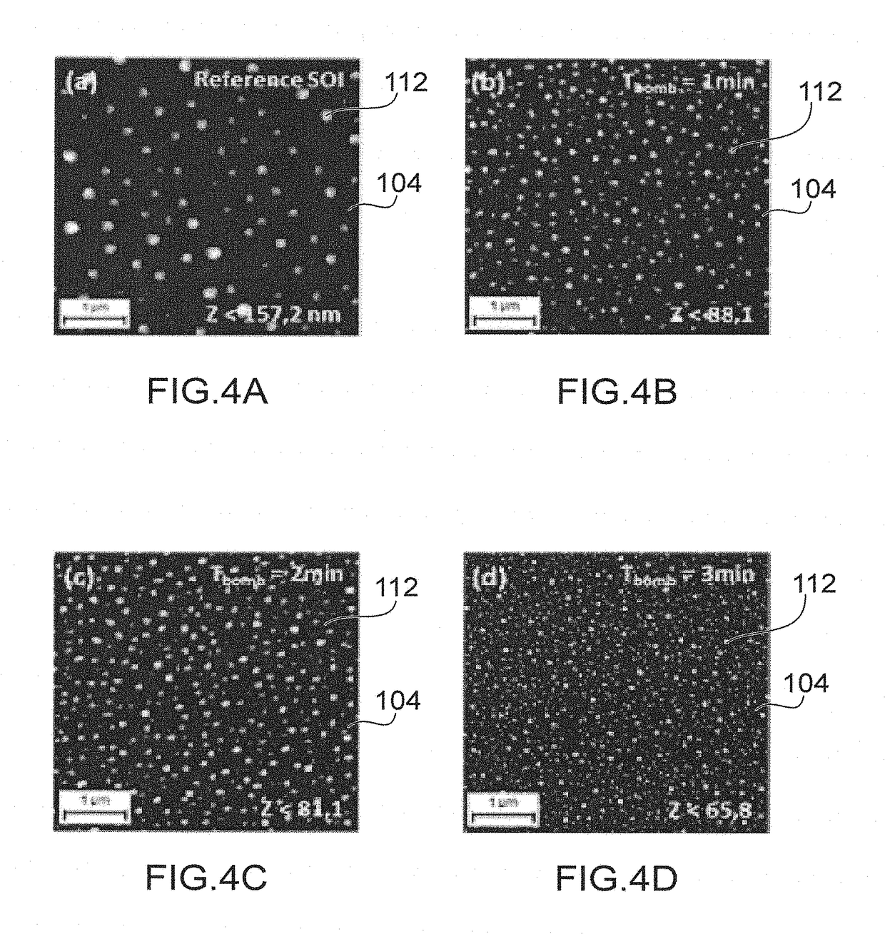
[0013]This method makes it possible to control the dimensions and the surface density of the nanocrystals obtained by dewetting. To do so, the method proposes controlling the dewetting thanks to a treatment of the thin layer of semiconductor by ion bombardment. The longer the duration of the ion bombardment, the smaller the dimensions of the nanocrystals obtained and the higher the surface density with which the nanocrystals are distributed on the dielectric layer. This method notably makes it possible to reduce the dimensions of the nanocrystals, and to obtain in particular nanoparticles of average diameter less than around 50 nm, without having to reduce, prior to the dewetting, the thickness of the thin layer, or to add carbon species to the thin layer of semiconductor or instead to induce stress in the semiconductor.

Problems solved by technology

This method nevertheless does not make it possible to act on the dimensions of the nanocrystals produced or on the distribution surface density of the nanocrystals.
Nevertheless, in practice, the reduction of the thickness of the thin layer of semiconductor poses difficulties of obtaining large homogeneous surfaces in terms of thickness, typically at the scale of the substrate or wafer (for example of diameter between 200 mm and 300 mm).
Such a method nevertheless does not make it possible to obtain particles of small dimensions, for example of average diameter less than around 50 nm.
The formation of carbon chemical species on the thin layer of semiconductor is nevertheless a restrictive step to implement, which may be incompatible with certain electronic applications.
Nevertheless, obtaining a stress in the semiconductor intended to be dewetted is restrictive and may be incompatible vis-à-vis other implementation stresses.
In addition, such an etching may be incompatible with certain envisaged applications.

Method used


Image

  • Method for producing nanocrystals with controlled dimensions and density
  • Method for producing nanocrystals with controlled dimensions and density
  • Method for producing nanocrystals with controlled dimensions and density

Examples


Embodiment Construction

[0009]There thus exists a need to propose a method for producing nanocrystals of semiconductor making it possible to reduce the dimensions of the nanocrystals and to increase the surface density with which the nanocrystals are distributed, which is notably compatible with obtaining nanocrystals of dimensions for example less than around 50 nm, without having to implement thinning of the thin layer of semiconductor to dewet to obtain a thickness that depends on the desired dimensions for the nanocrystals, add carbon species to the thin layer of semiconductor or induce a stress in the thin layer of semiconductor.

[0010]To do so, an embodiment proposes a method for producing nanocrystals, or nanoparticles, of semiconductor, comprising at least the implementation of the following steps:[0011]ion bombardment, or implantation, of a thin layer of semiconductor arranged on at least one dielectric layer, achieving an implantation of ions of at least one chemical element of rare gas type and / o...


PUM

PropertyMeasurementUnit
pressureaaaaaaaaaa
thicknessaaaaaaaaaa
thicknessaaaaaaaaaa

Abstract

Method for producing nanocrystals of semiconductor, comprising at least:ion bombardment of a thin layer of semiconductor arranged on at least one dielectric layer, achieving at least one among an implantation of ions of at least one chemical element of rare gas type and an implantation of ions of at least one semiconductor element of same nature as that of the thin layer, in at least one part of the thickness of the thin layer;annealing of the thin layer achieving a dewetting of the semiconductor of the thin layer and forming, on the dielectric layer, nanocrystals of semiconductor.

Description

TECHNICAL FIELD AND PRIOR ART[0001]The present document relates to a method for producing nanocrystals, or nanoparticles, of semiconductor obtained by dewetting of a thin layer of semiconductor arranged on a dielectric layer, and being able to be used for the production of microelectronic and / or nanoelectronic devices, for example memory devices or light emitting devices of LED type, or the production of holes or vias of controlled dimensions, distributed for example in the form of a quasi-periodical array, obtained thanks to a chemical reaction between the nanocrystals of semiconductor and the dielectric layer on which the nanocrystals are produced. This also applies to the formation of nano-catalyst particles such as carbon nanotubes, or the adaptation of surface wetting properties used for example to produce super-hydrophobic surfaces.[0002]It is known to produce nanocrystals of semiconductor, that is to say aggregates of semiconductor of which the dimensions may be between aroun...

Claims


Application Information

Patent Timeline
Patent Type & Authority Patents(United States)
IPC IPC(8): H01L21/02H01L21/324H01L21/265
CPCH01L21/02694H01L21/02381H01L21/02488H01L21/02532H01L21/324H01L21/02601H01L21/02664H01L21/26506H01L21/02598
Inventor ALMADORI, YANNBARBE, JEAN-CHARLESBOROWIK, LUKASZ
Owner COMMISSARIAT A LENERGIE ATOMIQUE ET AUX ENERGIES ALTERNATIVES
Learn More