Test circuit for memory device and semiconductor integrated device including the test circuit

a test circuit and memory device technology, applied in the direction of information storage, static storage, instruments, etc., can solve the problems of increasing the test cost, and requiring a period of several tens of times longer, so as to achieve efficient execution and efficient execution

Active Publication Date: 2018-11-13
MEGACHIPS
View PDF10 Cites 0 Cited by
  • Summary
  • Abstract
  • Description
  • Claims
  • Application Information

AI Technical Summary

Benefits of technology

[0011]In view of the circumstances descried above, an object of the present invention is to provide a test circuit capable of efficiently testing a nonvolatile memory combined with other parts and incorporated in a semiconductor integrated device, such as an ASIC.
[0012]More specifically, an object of the present invention is to provide a test circuit capable of efficiently testing a semiconductor integrated device including a flash memory under minimum control of a tester.
[0027]According to the present invention, a test for a nonvolatile memory mounted together with a logic chip on a semiconductor integrated device can be efficiently executed.
[0028]Further, according to the present invention, a test for a semiconductor integrated device including a flash memory that varies in terms of specifications on a vender basis and a model basis can be efficiently executed under minimum control of a tester.

Problems solved by technology

Read / write operation performed on a flash memory, however, typically requires a period several tens of times longer than in a case of the other memory devices, such as a DRAM.
Therefore, executing different tests in a sequential manner, as described in Patent Document 1, undesirably requires a long period until all the tests are completed, resulting in an increase in the test cost.
Therefore, to test a flash memory, it is necessary to prepare a test sequence based on a variety of parameters and commands on a memory vender basis and a model basis, resulting in an increase in the test cost.

Method used


Image

  • Test circuit for memory device and semiconductor integrated device including the test circuit
  • Test circuit for memory device and semiconductor integrated device including the test circuit
  • Test circuit for memory device and semiconductor integrated device including the test circuit

Examples


Embodiment Construction

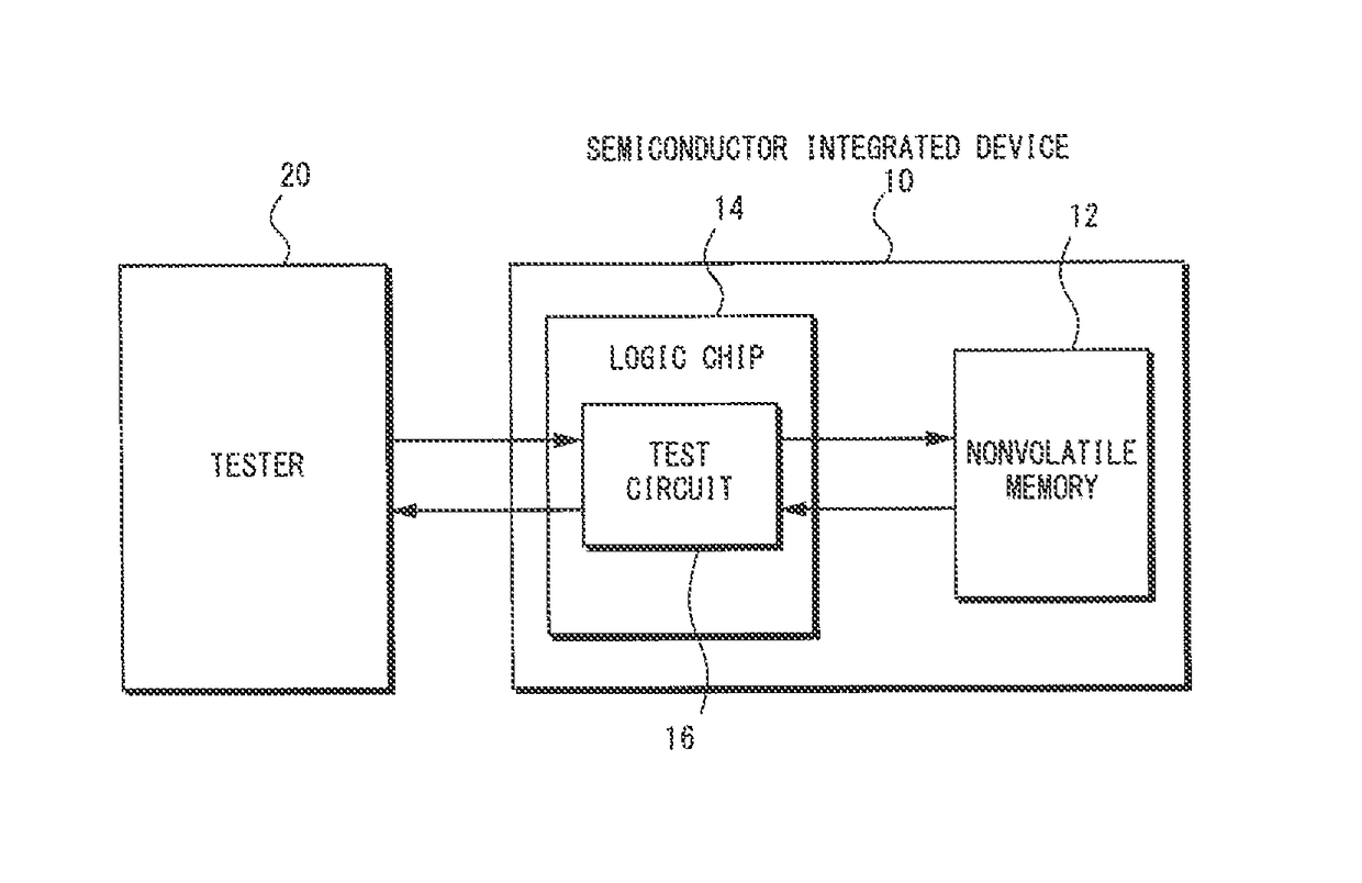
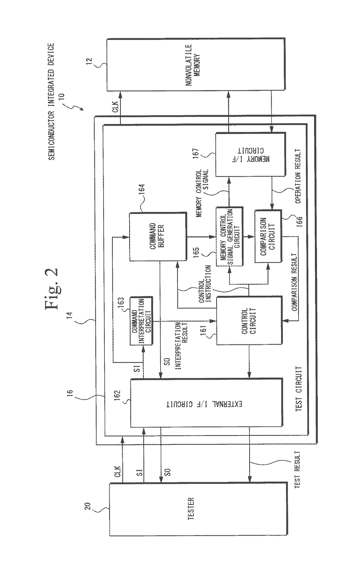
[0037]An embodiment of the present invention will be described below with reference to the drawings. It is, however, noted that the embodiment described below is presented only by way of example, and it is not intended to exclude a variety of changes and technology applications that are not explicitly described below. The present invention can be implemented in a variety of variations (e.g., combination of embodiments) to the extent that they do not depart from the substance of the present invention. Further, in the illustration in the following drawings, the same or similar portion has the same or similar reference character. The drawings are schematically drawn, and the dimensions, ratios, and other factors in the drawings do not necessarily coincide with actual dimensions, ratios, and other factors. Also in some figures, some portions may be drawn in a dimension ratio and other ratios different from the actual dimension ratio and other ratios.

[0038]The present embodiment disclose...


PUM


Abstract

An efficient test for a flash memory combined with a logic chip and incorporated in a semiconductor integrated device can be executed.A logic chip combined with a rewritable nonvolatile memory and incorporated in a semiconductor integrated device is provided with a test circuit. The test circuit reads a programmable test sequence transmitted from an external tester and stored, generates a memory control signal specific to the nonvolatile memory in accordance with a product ID read on the basis of the test sequence, executes a test in which the generated memory control signal is outputted to the nonvolatile memory, and outputs, to the tester, a test result based on a value outputted from the nonvolatile memory in response to the memory control signal.

Description

BACKGROUND OF THE INVENTION[0001]Field of the Invention[0002]The present invention relates generally to test circuits for a memory device and a semiconductor integrated device including the test circuit, and particularly to a test circuit for a flash memory and a semiconductor integrated device that incorporates the flash memory and the test circuit combined therein, such as an ASIC.[0003]Description of the Related Art[0004]As the capacity and speed of an LSI chip increase, a cost required to test the LSI chip increases more and more. A test facilitating technology called BIST (built-in self test), in which part of a tester function of testing an LSI chip is incorporated as a test circuit in the LSI chip, is employed as an attempt to lower the test cost.[0005]For example, Patent Document 1 (Japanese Patent Application Publication No. 2003-077296) discloses a multichip-package (MCP) semiconductor device in which a logic chip and a memory chip are incorporated in a common package. The...

Claims


Application Information

Patent Timeline
Patent Type & Authority Patents(United States)
IPC IPC(8): G11C29/00G11C29/48G11C16/10G11C16/26G11C29/56G11C29/16
CPCG11C29/48G11C16/10G11C16/26G11C29/56004G11C29/56008G11C29/16G11C2029/5602
Inventor INOUE, HIDEFUMI
Owner MEGACHIPS
Why Eureka
Try Eureka