Circuit carrier and a method for producing a circuit carrier

a technology of circuit carrier and circuit, which is applied in the direction of printed circuit aspects, conductive pattern formation, electric connection formation of printed elements, etc., can solve the problems of many known connection techniques not being employed, and welding not being possibl

Active Publication Date: 2018-11-13
ROBERT BOSCH GMBH
View PDF5 Cites 0 Cited by
  • Summary
  • Abstract
  • Description
  • Claims
  • Application Information

AI Technical Summary

Benefits of technology

[0011]In one advantageous configuration of the method according to the invention, the raw material layer may be configured to be higher than the inserted part, wherein the shaped hole may be filled up after the insertion of the inserted part with a filler material which is vaporized while the thermal process is being carried out. In this way, it is advantageously possible to prevent the raw material of the substrate layer flowing over the inserted part and reducing the effective contact area.

Problems solved by technology

For the production of electrical terminals as outer contacts, which lead out from the substrate, thin conductive tracks on inorganic circuit carriers have the problem that many known connection techniques cannot be employed.
For example, welding is not possible because there is too little remeltable material in the contacts.

Method used


Image

  • Circuit carrier and a method for producing a circuit carrier
  • Circuit carrier and a method for producing a circuit carrier
  • Circuit carrier and a method for producing a circuit carrier

Examples


Embodiment Construction

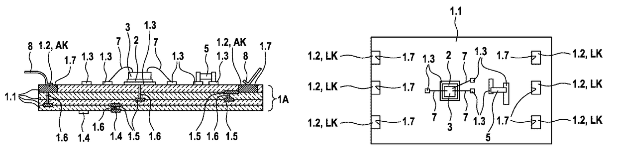
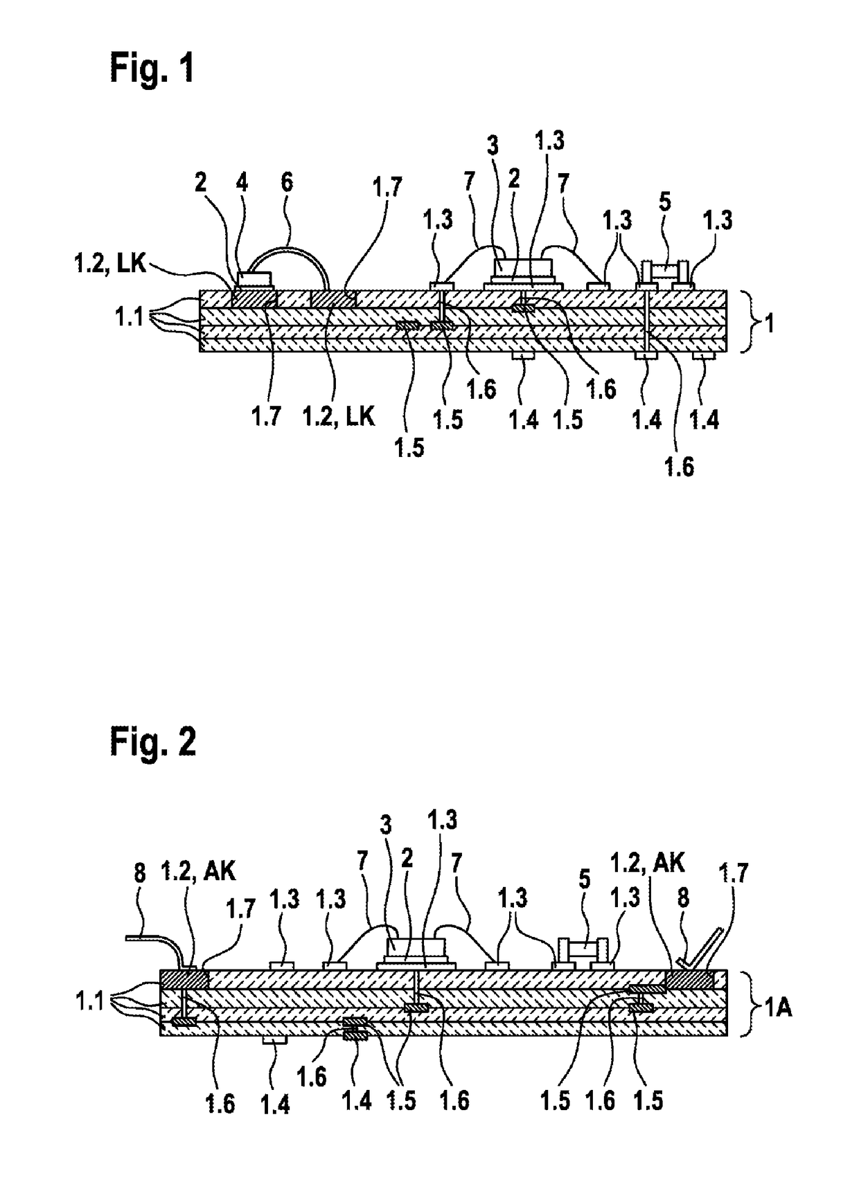
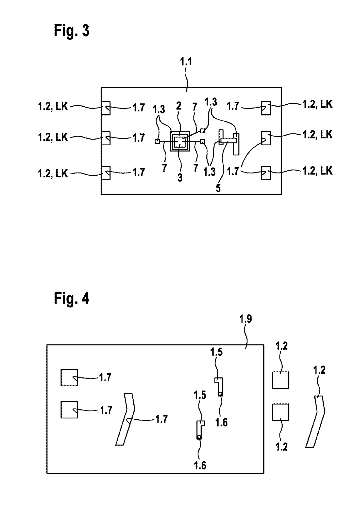
[0020]As can be seen from FIGS. 1 to 3, the represented exemplary embodiments of circuit carriers 1, 1A according to the invention respectively comprise a plurality of inorganic substrate layers 1.1 that have partial metallizations 1.2, 1.3, 1.4, 1.5, 1.6 for electrical and / or thermal conduction. According to the invention, at least one partial metallization is configured as an inserted part 1.2 which fills a corresponding shaped hole 1.7 that is introduced into one of the inorganic substrate layers 1.1.

[0021]The circuit carriers 1, 1A represented in FIGS. 1 to 3 respectively show an exemplary embodiment with four inorganic substrate layers 1.1, which are preferably configured as LTCC substrate layers. Of course, alternative exemplary embodiments of the circuit carrier according to the invention may also comprise more or fewer than four inorganic substrate layers. On the circuit carriers 1, 1A, in the exemplary embodiments represented, there are respectively a logic circuit 3 and a ...


PUM


Abstract

The invention relates to a circuit carrier (1) comprising a plurality of inorganic substrate layers (1.1) that have partial metallizations (1.2, 1.3, 1.4, 1.5, 1.6) for the purpose of electrical and / or thermal conduction, and to a corresponding method for producing such a circuit carrier (1). According to the invention, at least one partial metallization is made in the form of an insert (1.2) that fills a corresponding shaped hole (1.7) introduced into one of said inorganic substrate layers (1.1).

Description

BACKGROUND OF THE INVENTION[0001]The invention relates to a circuit carrier and to a method for producing a circuit carrier.[0002]Inorganic circuit carriers, for example low-temperature cofired ceramics (LTCC) are employed primarily as circuit carriers for logic circuits and relatively low circuit powers for use at high temperatures (up to about 300° C.). In the case of heavy currents of more than 20 A to be switched, in the case of conventional layer thicknesses in the range of from 1 to 20 μm, sometimes up to 100 μm, conductive tracks are very wide in order to cause little local intrinsic eating. The intrinsic heating is partly also increased because, in the case of inorganic circuit carriers (for example LTCC technology), metal / glass mixtures with increased resistivity are also used for the production of conductive tracks.[0003]For the production of electrical terminals as outer contacts, which lead out from the substrate, thin conductive tracks on inorganic circuit carriers have...

Claims


Application Information

Patent Timeline
Patent Type & Authority Patents(United States)
IPC IPC(8): H05K1/03H05K1/11H05K3/40H05K3/46H05K3/10H05K1/02
CPCH05K3/4629H05K1/0206H05K1/115H05K3/4046H05K2201/10416H05K1/0204H05K2201/0376
Inventor BUEYUEKGOEZ, HARUNGERSTNER, ROLANDWEBER, JOSEF
Owner ROBERT BOSCH GMBH
Why Eureka
Try Eureka