Circuit board bypass assemblies and components therefor

a circuit board bypass and circuit board technology, applied in the direction of coupling device connection, support structure mounting, instruments, etc., can solve the problems of reducing affecting so as to improve the emi performance of the connector port, remove the problem of signal integrity and impedance discontinuity, and create noise and impedance problems

Active Publication Date: 2018-11-20
MOLEX INC
View PDF362 Cites 18 Cited by
  • Summary
  • Abstract
  • Description
  • Claims
  • Application Information

AI Technical Summary

Benefits of technology

[0011]The chip package may include a plurality of contacts in the form of solder balls disposed on the underside of a chip package for providing connections to and from logic, clock, power and low-speed and high speed signal circuits to traces on the motherboard of a device in which the chip package is used. The contacts associated with the high speed signal circuits of the chip are removed from the bottom of the chip package inasmuch as the high speed traces are no longer routed to the bottom of the chip package. Some traces of the chip package may continue to be routed to the bottom of the package such as clock signals, logic signals, low speed signals and power. The termination locations for these traces are easily routed on the top of the chip package substrate where they can be easily connected to cables in a manner that maintains the geometry of the cable signal transmission lines. The high speed signal traces of the chip package are no longer routed through plated through holes, micro-vias, solder balls or a multilayer circuit board. Such a bypass assembly removes the signal transmission lines from the motherboard, not only alleviating the loss and noise problems referred to above, but also freeing up considerable space (i.e., real estate) on the motherboard, while permitting low cost circuit board materials, such as FR4, to be used for its construction.
[0021]All of the components can be combined together in a manner so that the cables, cable-direct connector, connector housing, heat transfer member and indicator light bar all cooperatively form an integrated assembly that may be connected directly to a chip package to define a high speed transmission channel assembly that does not utilize lossy traces on a circuit board. Such a transmission channel assembly may also include a preselected chip in the chip package so that the entire assembly can be plugged into a host device after the bulk of the device has been fabricated. The use of integrated assemblies such as those described herein reduces the number of assembly steps and the cost of manufacturing of the host devices.

Problems solved by technology

Although inexpensive, FR4 is known to be lossy in high speed signal transmission lines which transfer data at rates of about 6 Gbps and greater (e.g., above 3 GHz signaling frequencies).
These losses increase as the frequency increases and therefore make FR4 material undesirable for the high speed data transfer applications at signaling frequencies of about 10 GHz and greater.
In order to use FR4 as a circuit board material for high frequency signal transmission lines, a designer may have to utilize amplifiers and equalizers, which increase the final cost of the device.
The overall length of the signal transmission lines in FR4 circuit boards can exceed threshold lengths, about 10 inches, and may include bends and turns that can create signal reflection and noise problems as well as additional losses.
Losses can sometimes be corrected by the use of amplifiers, repeaters and equalizers but these elements also increase the cost of manufacturing the final circuit board.
This complicates the layout of the circuit board as additional board space is needed to accommodate these amplifiers and repeaters.
These turns and the transitions which occur at termination points along the signal transmission lines may negatively affect the integrity of the signals transmitted thereby.
It then becomes difficult to route transmission line traces in a manner to achieve a consistent impedance and a low signal loss therethrough.
Custom materials, such as Megtron, are available for circuit board construction which that reduce such losses, but the prices of these materials severely increase the cost of the circuit board and, consequently, the electronic devices in which they are used.
FR4 circuit board materials can handle data transmission speeds of 10 Gbits / sec, but this handling comes with disadvantages.
Increased power is required to transmit signals over longer trace lengths, so designers find it difficult to provide “green” designs, as low power chips cannot effectively drive signals for such lengths.
The higher power needed to drive the high speed signals over these lengths consumes more electricity and generates more heat that must be dissipated.
Accordingly, these disadvantages further complicate the use of FR4 as a motherboard material used in electronic devices.
Using more expensive, and exotic motherboard materials, such as Megtron, to handle the high speed signals at more acceptable losses increases the overall cost of electronic devices.
Notwithstanding the low losses experienced with these expensive materials, they still require increased power to transmit their signals and incurred, and the turns and crossovers required in the design of lengthy board traces create areas of signal reflection and potential increased noise.
This type of connection permits unobstructed airflow through an associated heat sink supported by the housing, furthers frees up space in the circuit board behind the housing, and saves cost in routing the mother board as the LEDs are no longer positioned behind, underneath or alongside the housing.
The placement of the LEDs without using light pipes or any sort of elongated light transmission member also reduces the likelihood of crosstalk from occurring.

Method used


Image

  • Circuit board bypass assemblies and components therefor
  • Circuit board bypass assemblies and components therefor
  • Circuit board bypass assemblies and components therefor

Examples


Embodiment Construction

[0080]The detailed description that follows describes exemplary embodiments and is not intended to be limited to the expressly disclosed combination(s). Therefore, unless otherwise noted, features disclosed herein may be combined together to form additional combinations that were not otherwise shown for purposes of brevity.

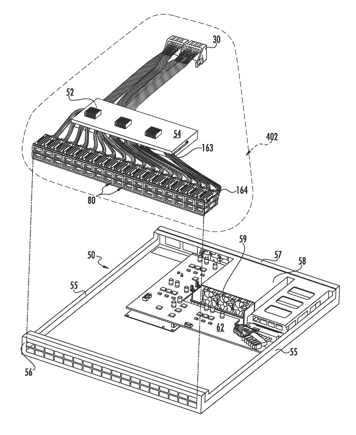
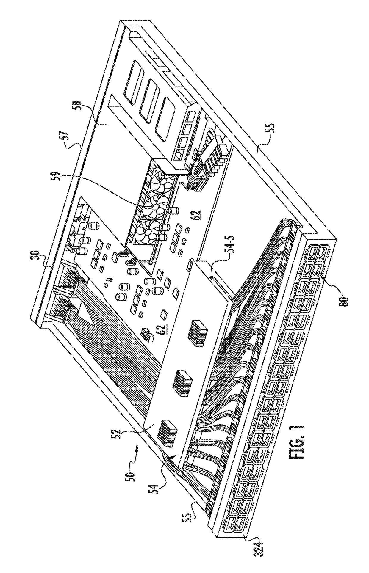
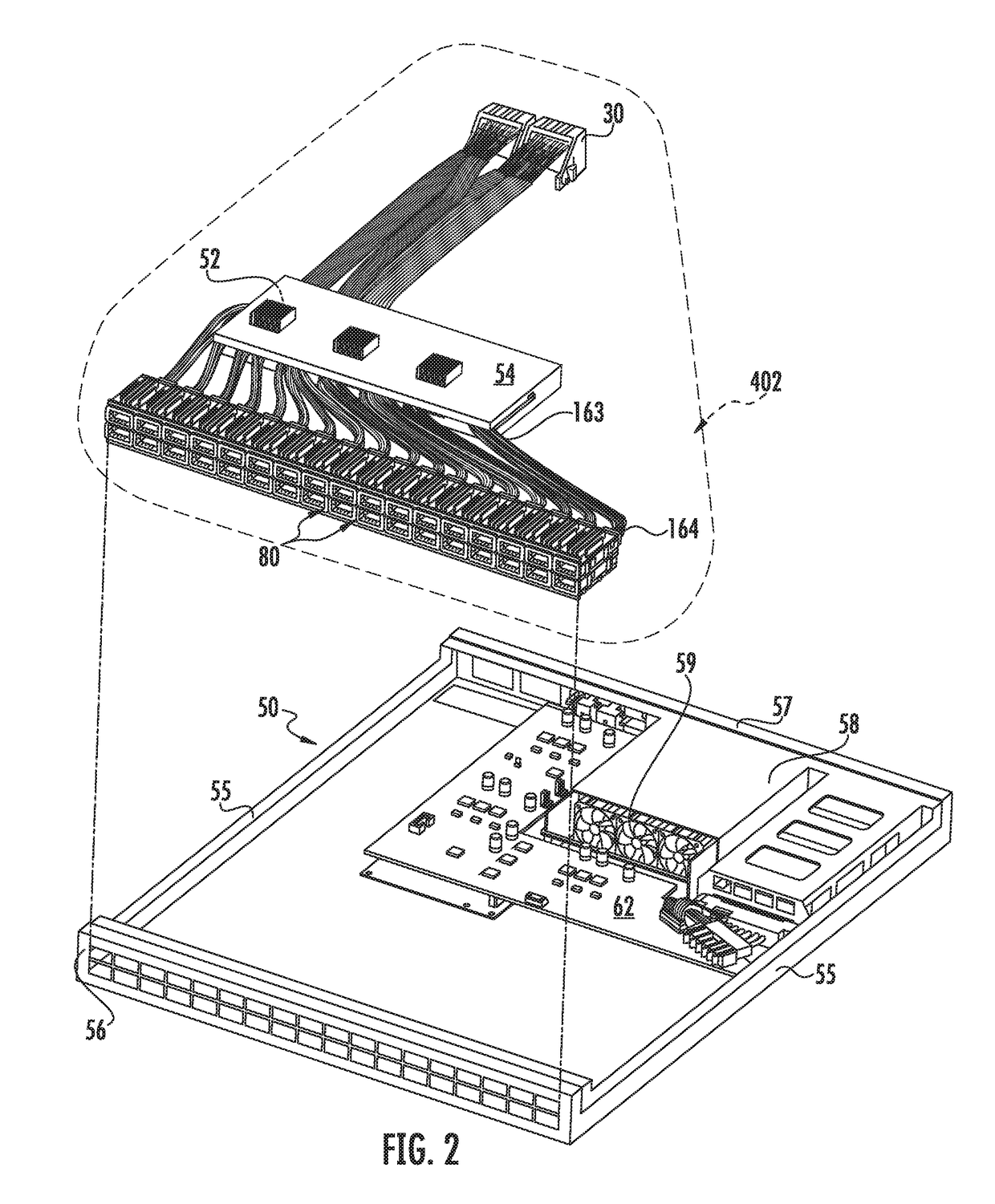
[0081]Accordingly, there is provided herein, an improved connector for use in a connector port that is connected directly to cables or wires, rather than traces on circuit boards to define signal transmission lines from the connector and directly to chips and processors of the host device, which are useful for high speed data applications at 10 Gbps and above and with low loss characteristics. Accordingly, the Present Disclosure is therefore directed to connectors and connector assemblies that are suitable for use in free standing external connector ports and which are directly connected to device components by cables, rather than use traces on circuit boards. The...


PUM


Abstract

A connector for use in a free-standing connector port for mating with an external pluggable module is disclosed. The connector has terminals that extend lengthwise of the connector so that cables may be terminated to the terminals and the terminals and cable generally are horizontally aligned together. The connector includes a housing and a pair of connecting elements that flank a card-receiving slot of the connector. The cables exit from the rear of the connector elements and from the connector port. The connector elements engage the connector port to fix the connector in place within the connector port.

Description

RELATED APPLICATIONS[0001]This application claims priority to International Application No. PCT / US2016 / 012848, filed Jan. 11, 2016, which in turn claims priority to prior U.S. provisional patent application No. 62 / 102,045, filed Jan. 11, 2015 entitled “The Molex Channel”; prior U.S. provisional patent application No. 62 / 102,046, filed Jan. 11, 2015 entitled “The Molex Channel”; prior U.S. provisional patent application No. 62 / 102,047, filed Jan. 11, 2015 entitled “The Molex Channel”; prior U.S. provisional patent application No. 62 / 102,048 filed Jan. 11, 2015 entitled “High Speed Data Transmission Channel Between Chip And External Interfaces Bypassing Circuit Boards”; prior U.S. provisional patent application No. 62 / 156,602, filed May 4, 2015, entitled “Free-Standing Module Port And Bypass Assemblies Using Same”, prior U.S. provisional patent application No. 62 / 156,708, filed May 4, 2015, entitled “Improved Cable-Direct Connector”; prior U.S. provisional patent application No. 62 / 15...

Claims


Application Information

Patent Timeline
Patent Type & Authority Patents(United States)
IPC IPC(8): H01R31/00H01R13/6583H01R13/717H01R24/60G06F1/18H05K7/14H01R13/66H01R12/79
CPCH01R31/005G06F1/181G06F1/189H01R12/79H05K7/1492H01R13/6658H01R13/7175H01R24/60H05K7/1487H01R13/6583H01R13/665H01L31/00
Inventor LLOYD, BRIAN KEITHWALZ, GREGORY B.REED, BRUCEFITZGERALD, GREGORYISAAC, AYMANREGNIER, KENT E.JANOWIAK, BRANDONSCHULZ, DARIAN R.AHMAD, MUNAWARJONES, ERAN J.RESENDEZ, JAVIERROST, MICHAEL
Owner MOLEX INC
Why Eureka
Try Eureka