Measurement of semiconductor structures with capillary condensation

a semiconductor structure and capillary condensation technology, applied in the field of metalrology systems and methods, can solve the problems of low measurement sensitivity to some parameters, errors in parameter value estimation, and multiple parameter models having a relatively large number of floating parameter values that are not computationally tractable, and achieve the effect of improving measurement contras

Active Publication Date: 2018-12-04
KLA CORP
View PDF51 Cites 8 Cited by
  • Summary
  • Abstract
  • Description
  • Claims
  • Application Information

AI Technical Summary

Benefits of technology

[0012]In some examples, multiple measurements of a structure are performed for different condensation states. Each measurement corresponds to a different amount of condensate condensed onto the structures under measurement. By collecting measurement signal information associated with a structure having geometric features filled with different amounts of condensate, parameter correlation among floating measurement parameters is reduced and measurement accuracy is improved.
[0018]In some embodiments, the fill material exhibits fluorescence in response to the illumination light provided to the structures under measurement to enhance measurement contrast, particularly in image based measurement applications.

Problems solved by technology

Complex, multiple parameter models include modeling errors induced by parameter correlations and low measurement sensitivity to some parameters.
In addition, regression of complex, multiple parameter models having a relatively large number of floating parameter values may not be computationally tractable.
Although fixing the values of a number of parameters may improve calculation speed and reduce the impact of parameter correlations, it also leads to errors in the estimates of parameter values.
Currently, the solution of complex, multiple parameter measurement models often requires an unsatisfactory compromise.
Moreover, complex, multiple parameter models make it difficult, or impossible, to optimize system parameter selections (e.g., wavelengths, angles of incidence, etc.) for each parameter of interest.
Future metrology applications present challenges due to increasingly small resolution requirements, multi-parameter correlation, increasingly complex geometric structures, and increasing use of opaque materials.

Method used


Image

  • Measurement of semiconductor structures with capillary condensation
  • Measurement of semiconductor structures with capillary condensation
  • Measurement of semiconductor structures with capillary condensation

Examples


Embodiment Construction

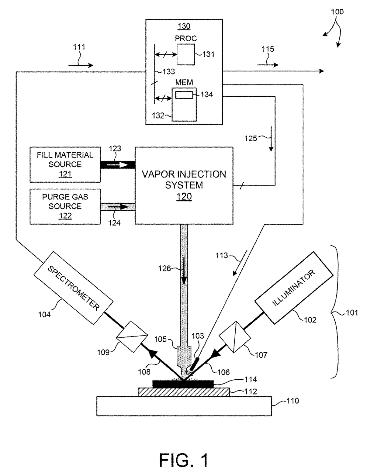
[0040]Reference will now be made in detail to background examples and some embodiments of the invention, examples of which are illustrated in the accompanying drawings.

[0041]Methods and systems for performing optical measurements of geometric structures filled with a condensate by a capillary condensation process are presented herein. Model based measurements are performed with an enriched data set including measurement signals collected from a metrology target having geometric features filled with a condensate. This reduces parameter correlation among floating measurement parameters and improves measurement accuracy. Thus, sufficiently accurate model-based measurement results can be obtained, and often with reduced computational effort.

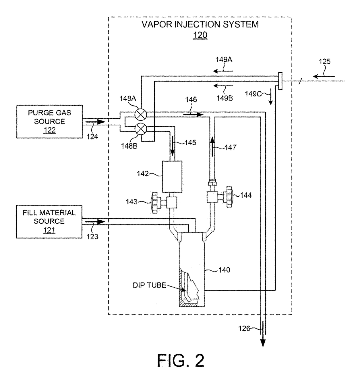
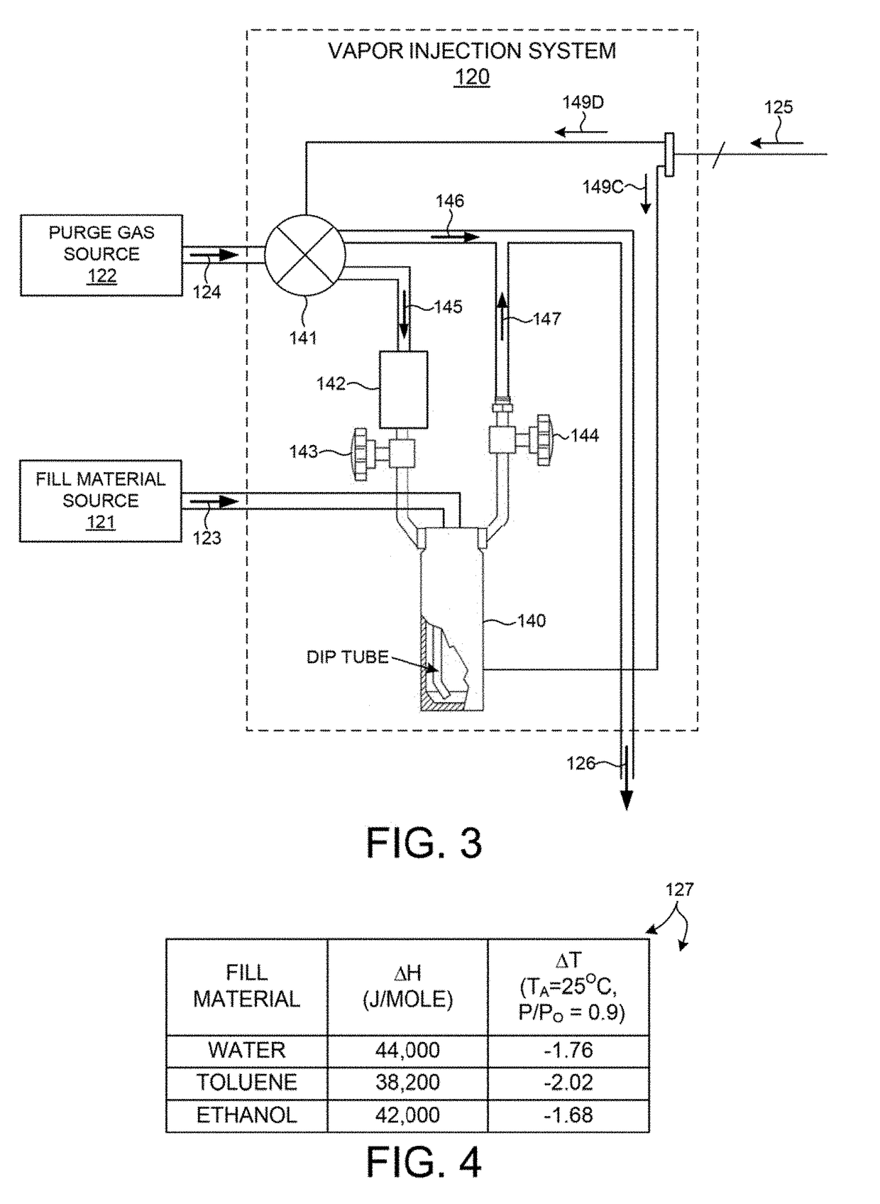
[0042]Measurements are performed while the local environment around the metrology target under measurement is treated with a flow of purge gas that includes a controlled amount of fill material. A portion of the fill material (i.e., the condensate) c...


PUM

PropertyMeasurementUnit
illumination wavelengthsaaaaaaaaaa
wavelength rangeaaaaaaaaaa
temperatureaaaaaaaaaa

Abstract

Methods and systems for performing optical measurements of geometric structures filled by a capillary condensation process are presented herein. Measurements are performed while the structures under measurement are treated with a flow of purge gas that includes a controlled amount of fill material. A portion of the fill material condenses onto the structures under measurement and fills openings in the structural features, spaces between structural features, small volumes such as notches, trenches, slits, contact holes, etc. The degree of saturation of vaporized material in the gaseous flow is adjusted based on the maximum feature size to be filled. In some examples, measurement data, such as spectroscopic data or image data, are collected when a structure is unfilled and when the structure is filled by capillary condensation. The collected data are combined to improve measurement performance.

Description

CROSS REFERENCE TO RELATED APPLICATION[0001]The present application for patent claims priority under 35 U.S.C. § 119 from U.S. provisional patent application Ser. No. 62 / 330,751, entitled “Porosity and Critical Dimension Measurements Using Capillary condensation,” filed May 2, 2016, and from U.S. provisional patent application Ser. No. 62 / 441,887, entitled “Critical Dimension Measurements Using Liquid Filling,” filed Jan. 3, 2017, and from U.S. patent application Ser. No. 15 / 204,938, entitled “Critical Dimension Measurements With Capillary Condensation,” filed Jul. 7, 2016, the subject matter of each is incorporated herein by reference in its entirety.TECHNICAL FIELD[0002]The described embodiments relate to metrology systems and methods, and more particularly to methods and systems for improved measurement of structures fabricated in the semiconductor industry.BACKGROUND INFORMATION[0003]Semiconductor devices such as logic and memory devices are typically fabricated by a sequence of...

Claims


Application Information

Patent Timeline
Patent Type & Authority Patents(United States)
IPC IPC(8): G01N21/00G03F7/00G01N1/28G01B11/02G01N21/64G01N21/25
CPCG01B11/02G01N1/28G03F7/00G01N21/64G01B2210/56G01N21/255G03F7/70616
Inventor KRISHNAN, SHANKAR
Owner KLA CORP
Why Eureka
Try Eureka