Micro-transfer printable electronic component

a technology of electronic components and micro-transfers, applied in the direction of basic electric elements, electric devices, solid-state devices, etc., can solve the problems of waste of material and processing costs, the performance of the above-mentioned technology is lower than the performance of the other integrated circuit, and the above-mentioned technology has some limitations, so as to achieve the effect of fewer process steps, simple and inexpensive electrical interconnection process

Active Publication Date: 2018-12-11
X DISPLAY CO TECH LTD
View PDF359 Cites 38 Cited by
  • Summary
  • Abstract
  • Description
  • Claims
  • Application Information

AI Technical Summary

Benefits of technology

[0030]Because the electronic components can be made using integrated circuit photolithographic techniques having a relatively high resolution and cost and the destination substrate, for example a printed circuit board, can be made using printed circuit board techniques having a relatively low resolution and cost, the contact pads on the destination substrate can be much larger than the connection posts or electrical contacts on the electronic component, facilitating the use of multiple connection posts with a common contact pads, reducing electrical faults, and reducing manufacturing costs.
[0038]The present invention provides structures and methods that enable the construction of light-emitting components that are transfer printed on a destination substrate. The electrical interconnection process is simple and inexpensive requiring fewer process steps than known alternative methods.

Problems solved by technology

The above techniques have some limitations.
Despite processing methods used to improve the performance of thin-film transistors, such transistors may provide performance that is lower than the performance of other integrated circuits (ICs) formed in mono-crystalline semiconductor material.
Semiconductor material and active components can be provided only on portions of the substrate, leading to wasted material and processing costs.
The choice of substrate materials can also be limited by the processing steps necessary to process the semiconductor material and the photo-lithographic steps used to pattern the active components.
For example, plastic substrates have a limited chemical and heat tolerance and do not readily survive photo-lithographic processing.
Furthermore, the manufacturing equipment used to process large substrates with thin-film circuitry is relatively expensive.
However, such substrate materials can be more expensive or difficult to process.
However, these techniques may be limited in the size of the integrated circuits that can be placed.
While this approach can provide substrates with the same performance as integrated circuits, the size of such substrates may be limited, for example, to a 12-inch diameter circle, and the wafers are relatively expensive compared to other substrate materials such as glass, polymer, or quartz.
However, the bonding technique and the processing equipment for the substrates to form the thin-film active components on large substrates can be relatively expensive.
This method may require etching a significant quantity of material, and may risk damaging the exposed TFT array.
These methods, however, may require the patterned deposition of adhesive on the object(s) or on the second substrate.
Moreover, the laser beam that irradiates the object may need to be shaped to match the shape of the object, and the laser abrasion can damage the object to be transferred.
Furthermore, the adhesive cure takes time, which may reduce the throughput of the manufacturing system.
This process is expensive and requires a number of manufacturing steps.
Moreover, the topographical structure of the small integrated circuits over the destination substrate renders the electrical connections problematic.
For example, it can be difficult to form a continuous conductor from the destination substrate to the small integrated circuit because of the differences in height over the surface between the small integrated circuits and the destination substrate.

Method used


Image

  • Micro-transfer printable electronic component
  • Micro-transfer printable electronic component
  • Micro-transfer printable electronic component

Examples


Embodiment Construction

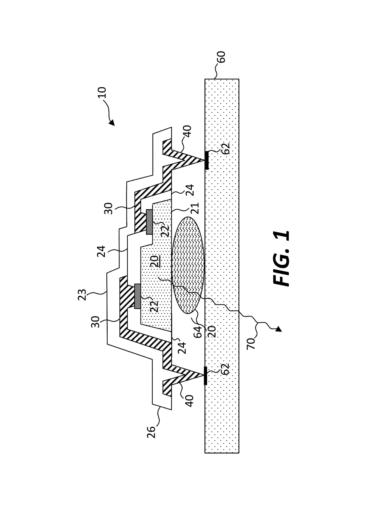
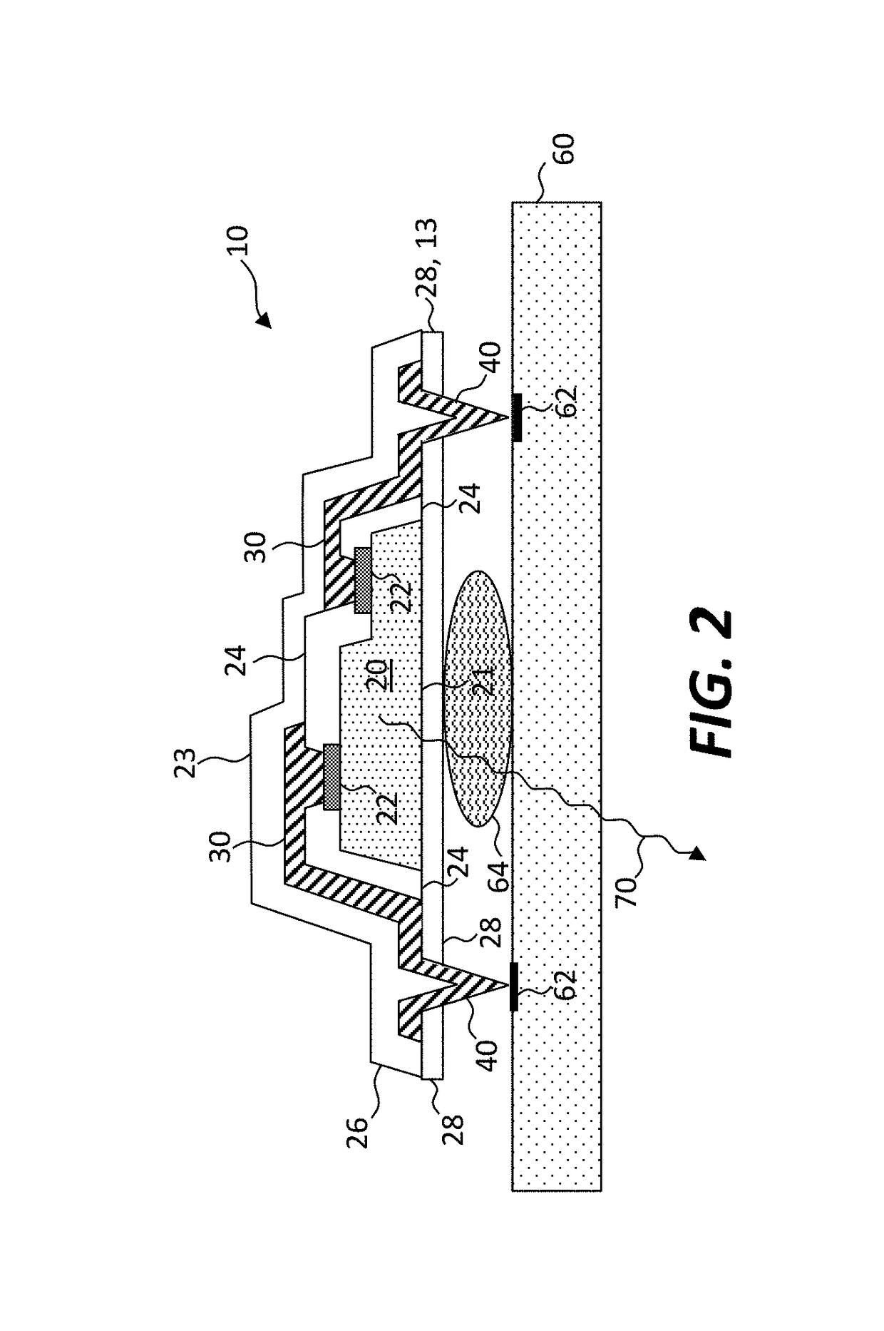
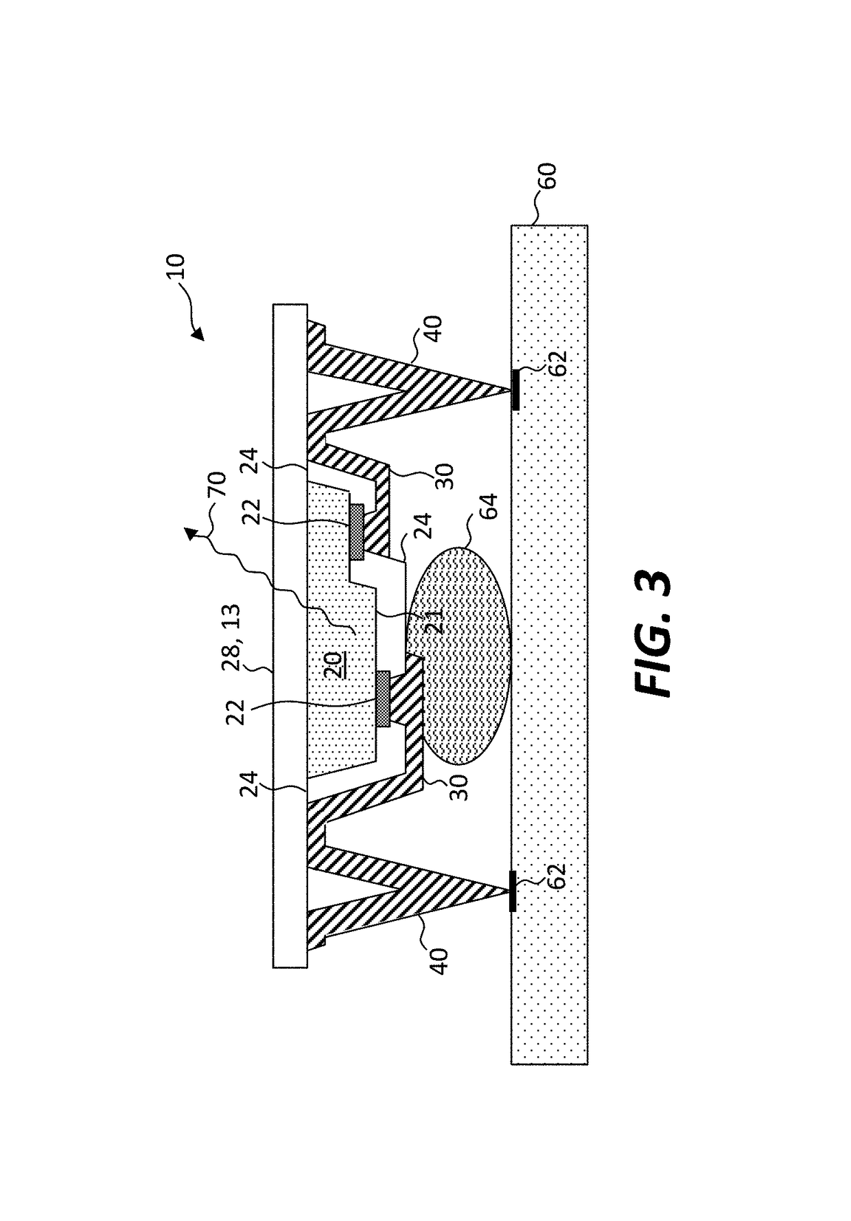
[0096]The present invention provides structures and methods for electrically connecting relatively small electronic devices such as integrated circuit chiplets or light-emitting diodes (LEDs) to a relatively large destination substrate in an efficient and cost-effective way and with fewer processing steps. Each micro-transfer printable electronic component can include a single integrated circuit, for example a digital circuit, an LED, a photo-diode, or a photo-transistor. Alternatively, the micro-transfer printable electronic component can include a circuit having multiple integrated circuits or other electronic or opto-electronic elements as well as electrically conductive wires interconnecting the multiple electronic elements to form a circuit on a component substrate. An electronic component can receive or provide electronic signals, but can also include electronic devices that have other modalities, such as optical elements, magnetic elements, electrical field elements, emission...


PUM


Abstract

A micro-transfer printable electronic component includes one or more electronic components, such as integrated circuits or LEDs. Each electronic component has device electrical contacts for providing electrical power to the electronic component and a post side. A plurality of electrical conductors includes at least one electrical conductor electrically connected to each of the device electrical contacts. One or more electrically conductive connection posts protrude beyond the post side. Each connection post is electrically connected to at least one of the electrical conductors. Additional connection posts can form electrical jumpers that electrically connect electrical conductors on a destination substrate to which the printable electronic component is micro-transfer printed. The printable electronic component can be a full-color pixel in a display.

Description

PRIORITY APPLICATION[0001]This application claims priority to U.S. Patent Application Ser. No. 62 / 303,096, entitled Micro-Transfer Printable LED Component, filed Mar. 3, 2016, the disclosure of which is incorporated herein by reference in its entirety.CROSS REFERENCE TO RELATED APPLICATION[0002]Reference is made to U.S. Pat. No. 8,889,485, entitled Methods for Surface Attachment of Flipped Active Components by Christopher Bower, filed Jun. 7, 2012, to U.S. patent application Ser. No. 14 / 822,868, entitled Compound Micro-Assembly Strategies and Devices by Bower et al., filed Aug. 10, 2015, and to U.S. patent application Ser. No. 14 / 822,864, entitled Chiplets with Connection Posts by Prevatte et al., filed Aug. 10, 2015, the disclosures of which are incorporated herein by reference in their entirety.FIELD OF THE INVENTION[0003]The present invention relates to structures and methods for electrically interconnecting light-emitting diodes to contact pads on a substrate using micro-transfe...

Claims


Application Information

Patent Timeline
Patent Type & Authority Patents(United States)
IPC IPC(8): H01L25/075H01L33/62H01L25/00H01L23/498H01L25/16H01L23/00
CPCH01L25/0753H01L23/49838H01L24/24H01L24/82H01L24/97H01L25/162H01L25/165H01L25/167H01L25/50H01L33/62H01L2924/13069H01L2924/14H01L2924/143H01L2924/1531H01L2924/1532H01L2924/15192H01L2924/1815H01L2224/97H01L2224/81H01L2924/18162H01L2224/04105H01L2224/24226H01L2224/24227H01L2224/32225H01L2224/73267H01L2224/82005H01L2924/10253H01L2924/12041H01L2924/12043H01L2924/12044
Inventor COK, RONALD S.BOWER, CHRISTOPHERMEITL, MATTHEWPREVATTE, JR., CARL
Owner X DISPLAY CO TECH LTD
Why Eureka
Try Eureka