
Method, circuit configuration and bridge circuit for charging a capacitance effective on main current terminals of semiconductor switch

a capacitance effective, semiconductor switch technology, applied in the direction of ac-dc conversion, electric pulse generator, electric variable regulation, etc., can solve the problems of high switching loss, transient overvoltage of semiconductor switch, significant switching loss, etc., to improve the utilization rate of semiconductor switch.

Active Publication Date: 2018-12-25
SEW-EURODRIVE GMBH & CO KG
View PDF15 Cites 0 Cited by
  • Summary
  • Abstract
  • Description
  • Claims
  • Application Information

AI Technical Summary

Benefits of technology

[0013]It is advantageous for this purpose that the reverse voltage load on the semiconductor switch is reduced without an increase in the switching losses. It is not necessary to take into account the power semiconductor topology and the pulse method for controlling the semiconductor switch, in particular in circuits having upper and lower switches such as, for example, bridge-circuits having a pulse-width modulated control. Example embodiments of the present invention may be used directly in switches of a hard-switching power semiconductor system and requires no significant inductances or capacitances in the load current circuit.
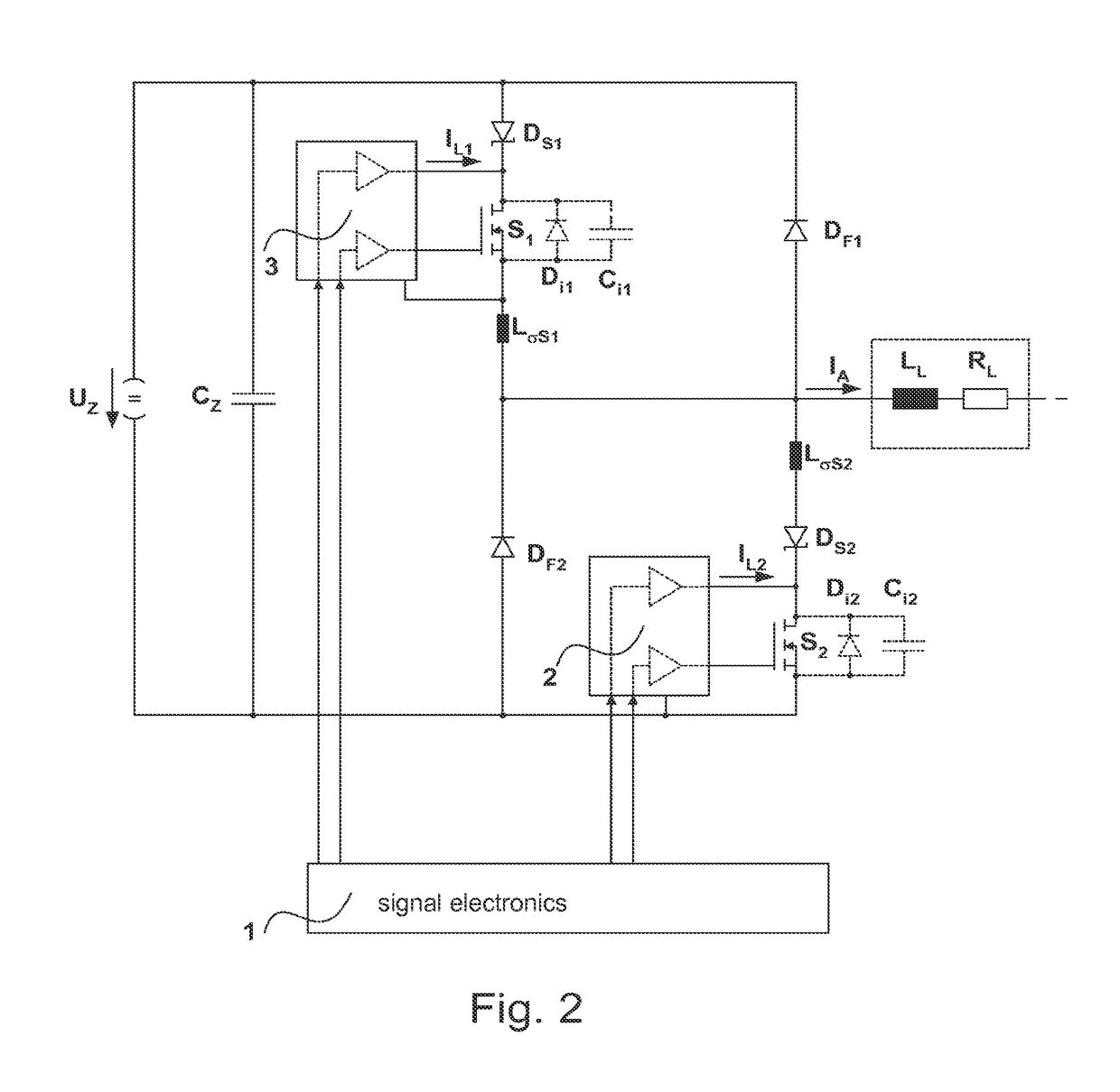
[0036]It is advantageous in this regard that overvoltages in bridge circuits are avoided because the additional transverse inductance increases the inductance normative for the above-mentioned series resonant circuit such that the amplitude of the ring-back current is decreased. The energy stored in the leakage inductances, which is restored into the drain-source capacitance, is thus also reduced such that the overvoltage is lower. The energy stored in the transverse inductance does not contribute to the overvoltage since it is converted into heat loss by the forward voltages of the free-wheeling diodes and semiconductor switches. This measure alone, that is, without the precharging of the drain-source capacitance, would indeed reduce the occurring overvoltages, but would also increase the conductive output losses in the semiconductor components. If this measure is combined with the precharging of the drain-source capacitance, however, then overvoltages are avoided and conductive output losses are reduced.LIST OF REFERENCE CHARACTERS

Problems solved by technology

The semiconductor switch is so to speak operated in its active range for the duration of the switching process, which can result in significant switching losses.
In MOSFET semiconductor switches, these diodes are intrinsically present and have great reverse currents and a correspondingly high reverse current chopping such that in systems that use these intrinsic diodes as free-wheeling diodes, high switching losses and transient overvoltages on the semiconductor switches occur.
Compared to the hard-switched converters, a higher switching expenditure is required in the resonance converters.
Often restrictions apply regarding the control methods.
However, the switch-on losses are increased compared to a circuit design having a fast recovery diode instead of the intrinsic diodes of the MOSFET semiconductor switches.
If the drain-source capacitance, however, decreases greatly with rising voltage, then the voltage may even overawing to many times the applied direct voltage.
The energy stored in the leakage inductance would subsequently have to be restored in a decreasing capacitance, which would cause an accordingly increased overvoltage on the drain-source capacitance.

Method used


Image

  • Method, circuit configuration and bridge circuit for charging a capacitance effective on main current terminals of semiconductor switch
  • Method, circuit configuration and bridge circuit for charging a capacitance effective on main current terminals of semiconductor switch
  • Method, circuit configuration and bridge circuit for charging a capacitance effective on main current terminals of semiconductor switch

Examples


case 1

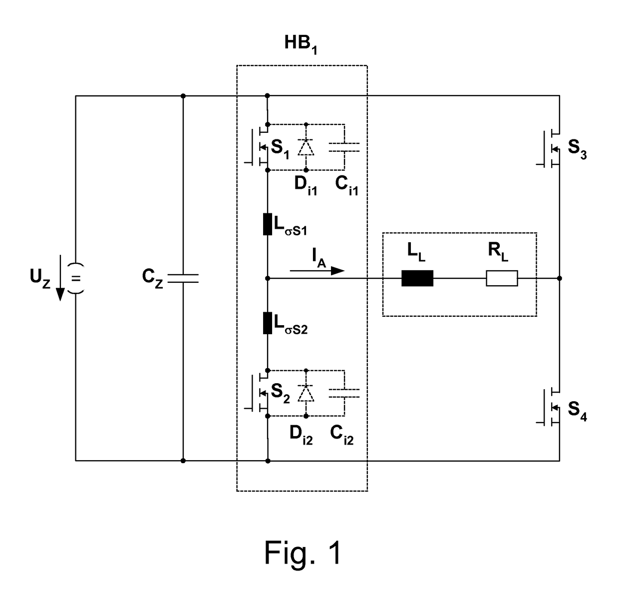
[0072]In the case of a negative load current IA, in state 1, the current flows via the closed semiconductor switch S2 to the negative terminal of supply voltage Uz. If the transition to state 2 is now initiated by switching S2 off, then drain-source capacitance CI2 is charged by the load current. The load current shall be assumed as constant during the commutation process. If drain-source voltage on CI2 reaches the value of the intermediate circuit voltage, then the load current would commutate abruptly and without transient overvoltage to free-wheeling diode Di1 if parasitic leakage inductances LσS1 and LσS2 did not exist. However, since the load current through LσS2 cannot diminish abruptly to zero, drain-source capacitance Ci2 continues to be charged until the energy stored in the leakage inductances has diminished to zero. The resulting overvoltage on S2 is thus a function of the magnitude of the load current, which is operationally limited to defined boundaries, however. Using ...


PUM


Abstract

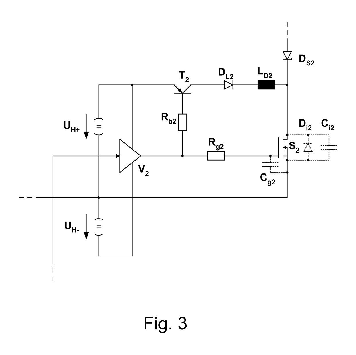
A method, circuit configuration and bridge circuit for charging a capacitance effective on the main current terminals of a semiconductor switch, in particular an intrinsic capacitance, in particular the drain-source capacitance of a MOSFET semiconductor switch or the collector-emitter capacitance of an IGBT semiconductor switch, the precharging, in particular the at least partial charging, of the effective capacitance being forcibly controlled via a charging current path.

Description

FIELD OF THE INVENTION[0001]The present invention relates to a method, a circuit configuration and a bridge circuit.BACKGROUND INFORMATION[0002]Circuit configurations in half-bridge circuit and full-bridge circuit are known for generating an alternating voltage from a direct voltage, which for example provide a potential-free direct voltage in switched-mode power supplies in combination with a downstream transformer having a rectifier.[0003]Three-phase or multiphase bridge circuits are also known for generating a multiphase alternating voltage, as are provided for example in frequency converters for the variable rotational speed adjustment of alternating current motors. Such converters for supplying power to electric motors are known to supply power to each motor supply line via a half-bridge of semiconductor switches, the half-bridges being supplied from a unipolar voltage, the so-called intermediate circuit voltage. The intermediate circuit voltage is produced by a mains-fed recti...

Claims


Application Information

Patent Timeline
Patent Type & Authority Patents(United States)
IPC IPC(8): H02M3/335H02M7/521
CPCH02M3/335H02M7/521
Inventor WOLF, HARALD
Owner SEW-EURODRIVE GMBH & CO KG
Learn More