Organic light emitting display device
a light-emitting display and organic technology, applied in the field of organic light-emitting display devices, can solve problems such as the decrease in the lifetime of the devi
- Summary
- Abstract
- Description
- Claims
- Application Information
AI Technical Summary
Benefits of technology
Problems solved by technology
Method used
Image
Examples
embodiment 1
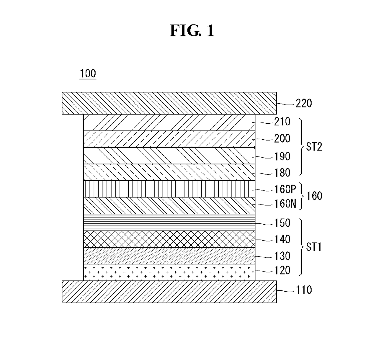
[0123]It has the same elements as the above-described Comparative Example 1, and the N-type charge generation layer was formed of Compound A.
[0124]
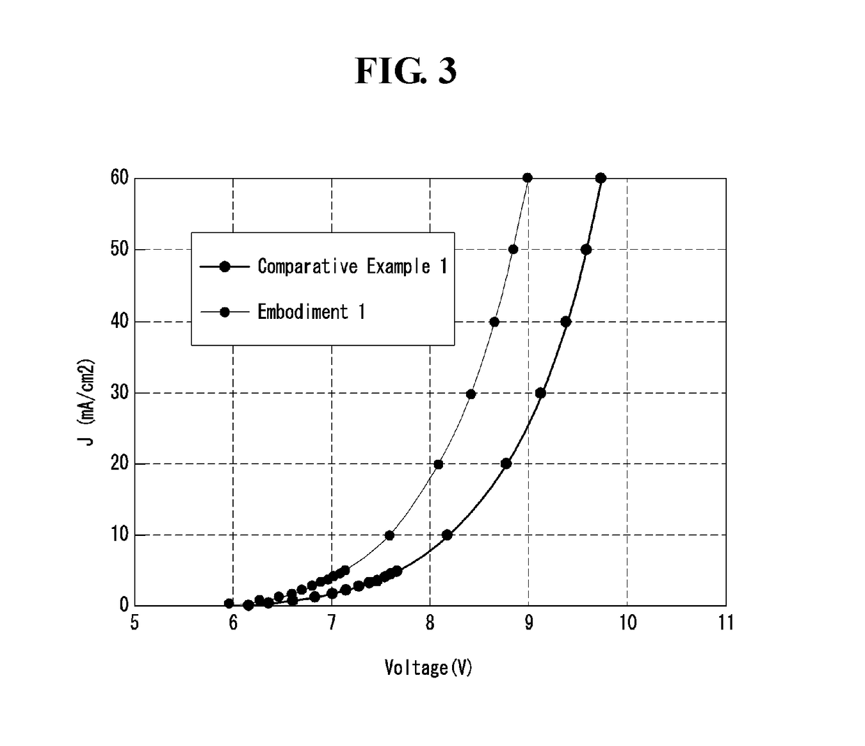
[0125]The operating voltage, light emission efficiency, external quantum efficiency, chromaticity coordinates, and lifetime of the devices manufactured according to the above-described Comparative Example 1 and Embodiment 1 of the present disclosure were measured and shown in the following Table 1. (The devices operated at a current density of 10 mA / cm2, lifetime T95 is white lifetime, which is the time it takes for the luminance to decrease to 95% of the initial luminance. The measurements taken in Embodiment 1 were expressed as a percentage relative to those taken in Comparative Example 1 corresponding to 100%).
[0126]The current density vs. operating voltage of the organic light emitting display devices manufactured according to Comparative Example 1 and Embodiment 1 was shown in FIG. 3, the light emission efficiency vs. luminance was s...
embodiment 2
[0132]It has the same elements as the above-described Comparative Example 1, and the N-type charge generation layer was formed of Compound B.
[0133]
[0134]The operating voltage, light emission efficiency, external quantum efficiency, chromaticity coordinates, and lifetime of the devices manufactured according to the above-described Comparative Example 2 and Embodiment 2 of the present disclosure were measured and shown in the following Table 2. The measurements taken in Embodiment 2 were expressed as a percentage relative to those taken in Comparative Example 2 corresponding to 100%.
[0135]The current density vs. operating voltage of the organic light emitting display devices manufactured according to Comparative Example 2 and Embodiment 2 was shown in FIG. 8, the light emission efficiency vs. luminance was shown in FIG. 9, the external quantum efficiency vs. luminance was shown in FIG. 10, the light emission spectra were shown in FIG. 11, and the rate of decrease in luminance over tim...
embodiment 3
[0141]It has the same elements as the above-described Comparative Example 1, and the N-type charge generation layer was formed of Compound C.
[0142]
[0143]The operating voltage, light emission efficiency, external quantum efficiency, chromaticity coordinates, and lifetime of the devices manufactured according to the above-described Comparative Example 3 and Embodiment 3 of the present disclosure were measured and shown in the following Table 3. The measurements taken in Embodiment 3 were expressed as a percentage relative to those taken in Comparative Example 3 corresponding to 100%.
[0144]The current density vs. operating voltage of the organic light emitting display devices manufactured according to Comparative Example 3 and Embodiment 3 was shown in FIG. 13, the external quantum efficiency vs. luminance was shown in FIG. 14, the light emission spectra were shown in FIG. 15, and the rate of decrease in luminance over time was shown in FIG. 16.
[0145]
TABLE 3LightExternalChromaticityLif...
PUM
| Property | Measurement | Unit |
|---|---|---|
| voltage | aaaaa | aaaaa |
| thickness | aaaaa | aaaaa |
| thickness | aaaaa | aaaaa |
Abstract
Description
Claims
Application Information


