Light emitting element, light emitting device, display, and electronic device
a technology of light emitting devices and light emitting elements, applied in the direction of thermoelectric devices, organic semiconductor devices, solid-state devices, etc., can solve the problems of increasing the current density, increasing the drive voltage, and deteriorating the transporting layer or the injecting layer of the hole, so as to achieve excellent reliability
- Summary
- Abstract
- Description
- Claims
- Application Information
AI Technical Summary
Benefits of technology
Problems solved by technology
Method used
Image
Examples
embodiment 1
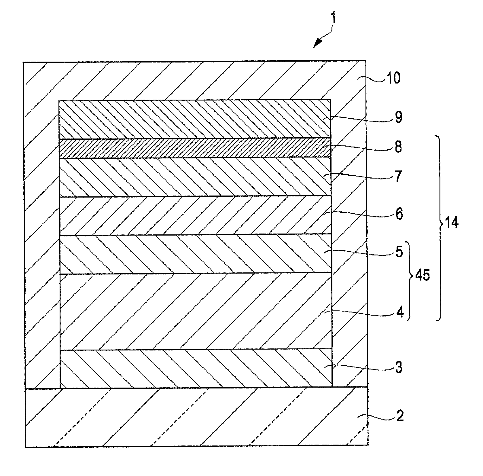
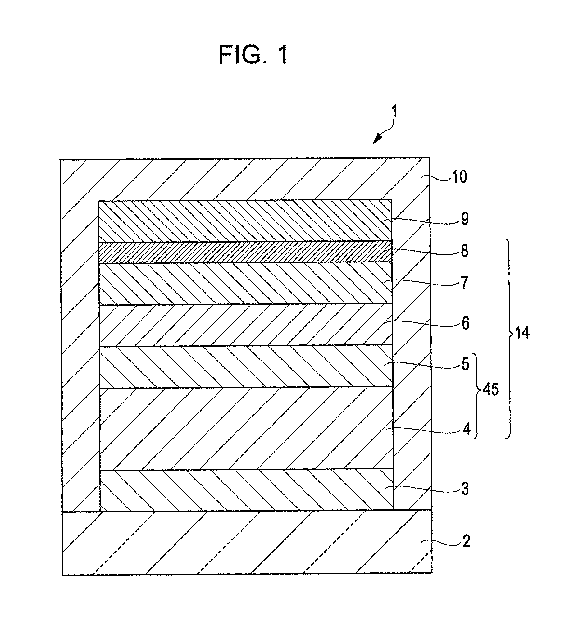
[0048]FIG. 1 is a cross sectional view schematically illustrating a light emitting element according to a first embodiment of the invention. The following description is given while defining the upper side of FIG. 1 as “top” and the lower side of FIG. 1 as “bottom” for convenience of explanation.
[0049]A light emitting element (electroluminescence element) 1 illustrated in FIG. 1 has a structure in which an anode 3, a hole injecting layer 4, a hole transporting layer 5, a light emitting layer 6, an electron transporting layer 7, an electron injecting layer 8, and a cathode 9 are laminated in this order. More specifically, in the light emitting element 1, a laminate 14 in which the hole injecting layer 4, the hole transporting layer 5, the light emitting layer 6, the electron transporting layer 7, and the electron injecting layer 8 are laminated in this order from the anode 3 side to the cathode 9 side is interposed between the anode 3 and the cathode 9. In this embodiment, a function...
example 1
[0211](1) First, a transparent glass substrate having an average thickness of 0.5 mm was prepared. Next, an ITO electrode (anode) having an average thickness of 150 nm was formed on the substrate by sputtering.
[0212]Then, the substrate was immersed in acetone, and then in 2-propanol for ultrasonic cleansing, followed by oxygen plasma treatment and argon plasma treatment. The plasma treatment was performed at a plasma power of 100 W, a gas flow rate of 20 sccm, and a treatment time of 5 sec in a state where the substrate was warmed to 70° C. to 90° C.
[0213](2) Next, the benzidine derivative (hole injecting material) represented by Formula (1) above and the anthracene derivative (electron transporting material) represented by Formula (10) above were co-deposited on the ITO electrode by vacuum vapor deposition, thereby forming a hole injecting layer having an average thickness of 50 nm.
[0214]Herein, the hole injecting layer was constituted by a mixed material of the benzidine derivativ...
example 2
[0226]A light emitting element was manufactured in the same manner as in Example 1 described above, except that the mixing ratio (weight ratio) of the benzidine derivative and the anthracene derivative in the hole injecting layer was (Benzidine derivative):(Anthracene derivative)=50:50.
PUM
 Abstract
Description
Claims
Application Information


