White organic electroluminescent device and preparation method thereof

a technology of electroluminescent devices and white organic materials, which is applied in the direction of luminescent compositions, organic semiconductor devices, luminescent compositions, etc., can solve the problems of low efficiency and brightness of devices, relatively high working voltage, and high manufacturing cost of devices, so as to improve light-emitting effectiveness improve spectral stability of devices. , the effect of improving the light-emitting effect of organic electroluminescent devices

Active Publication Date: 2019-01-08
CHANGCHUN INST OF APPLIED CHEMISTRY - CHINESE ACAD OF SCI
View PDF23 Cites 2 Cited by
  • Summary
  • Abstract
  • Description
  • Claims
  • Application Information

AI Technical Summary

Benefits of technology

[0039]In this application, by adding one or two of tris(acetylacetone)phenanthroline thulium and tris(acetylacetone)phenanthroline dysprosium to the electron-dominated light-emitting layer as an organic sensitive material. Since the energy level and the triplet energy thereof match the energy levels and the triplet energies of the electron-type host material and the blue light-emitting material, so that the organic sensitive material has the function of an energy transporting ladder and a deep binding center for charge carriers in the process of electroluminescence. This not only improves the energy transfer from the host material to the light-emitting material, but also balances the distribution of electrons and holes in the range of light emission. Therefore, the light-emitting effectiveness of the organic electroluminescent device is improved, the spectral stability of the device is improved, the operating voltage of the device is reduced, the efficiency attenuation of the device is delayed, and the service life of the device is improved.

Problems solved by technology

Although that device exhibits relatively ideal white light emission, the device has relatively low efficiency and brightness and relatively high working voltage, due to unbalanced carrier injection.
Additionally, complex structure of the device further results in relatively high manufacturing cost of the device
That device has relatively high light-emitting effectiveness, but the feature of double-peak emission results in that the spectrum of the device does not have enough coverage degree in the white-light region, and thus the color restoration coefficient is relatively low.
As thus can be seen, the overall properties, such as light-emitting effectiveness, brightness, spectral stability, service life, and the like, of the white organic electroluminescent device are still not effectively improved.

Method used


Image

  • White organic electroluminescent device and preparation method thereof
  • White organic electroluminescent device and preparation method thereof
  • White organic electroluminescent device and preparation method thereof

Examples


example 1

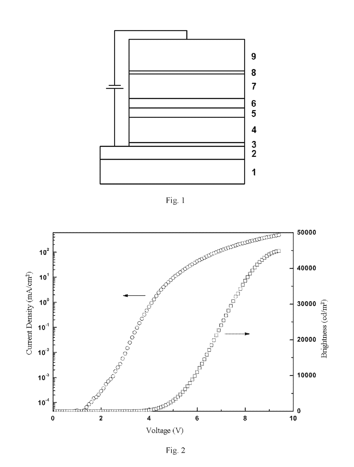
[0092]An ITO anode layer on an ITO glass was laser-etched into a strip electrode, then ultrasonically cleaned sequentially with a cleaning liquid and deionized water for 15 min. and placed in an oven for drying. The dried substrate was then placed in a pretreating vacuum chamber, and the ITO anode was subjected to a low-pressure plasma treatment for 3 min under an atmosphere having a vacuum degree of 10 Pa with a voltage of 400V and then transferred to an organic evaporation plating chamber. In an organic evaporation plating chamber with a vacuum degree of 1-2×10⁻⁵ Pa, a MoO3 anode modification layer 3 having a thickness of 3 nm, a TAPC hole transporting-electron blocking layer 4 having a thickness of 40 nm, a TcTa hole-dominated light-emitting layer 5 doped with PQ2Ir(dpm) and Ir(ppy)3 having a thickness of 10 nm, a CzSi electron-dominated light-emitting layer 6 co-doped with Tm(acac)3phen and FCNIrpic having a thickness of 10 nm, and a TmPyPB hole blocking-electron transporting la...

example 2

[0096]An ITO anode layer on an ITO glass was laser-etched into a strip electrode, then ultrasonically cleaned sequentially with a cleaning liquid and deionized water for 15 min, and placed in an oven for drying. The dried substrate was then placed in a pretreating vacuum chamber, and the ITO anode was subjected to a low-pressure plasma treatment for 3 min under an atmosphere having a vacuum degree of 10 Pa with a voltage of 400V and then transferred to an organic evaporation plating chamber. In an organic evaporation plating chamber with a vacuum degree of 1-2×10⁻⁵ Pa, a MoO3 anode modification layer 3 having a thickness of 3 nm, a TAPC hole transporting-electron blocking layer 4 having a thickness of 40 nm, a mCP hole-dominated light-emitting layer 5 doped with PQ2Ir(dpm) and Ir(ppy)3 having a thickness of 10 nm, a CzSi electron-dominated light-emitting layer 6 co-doped with Tm(acac)3phen and FCNIrpic having a thickness of 10 nm, and a TmPyPB hole blocking-electron transporting lay...

example 3

[0098]An ITO anode layer on an ITO glass was laser-etched into a strip electrode, then ultrasonically cleaned sequentially with a cleaning liquid and deionized water for 15 min, and placed in an oven for drying. The dried substrate was then placed in a pretreating vacuum chamber, and the ITO anode was subjected to a low-pressure plasma treatment for 3 min under an atmosphere having a vacuum degree of 10 Pa with a voltage of 400V and then transferred to an organic evaporation plating chamber. In an organic evaporation plating chamber with a vacuum degree of 1-2×10⁻⁵ Pa, a MoO3 anode modification layer 3 having a thickness of 3 nm, a TAPC hole transporting-electron blocking layer 4 having a thickness of 40 nm, a TcTa hole-dominated light-emitting layer 5 doped with PQ2Ir(dpm) and Ir(ppv)3 having a thickness of 10 nm, a 26DCzPPy electron-dominated light-emitting layer 6 co-doped with Dy(acac)3 and FCNIrpic having a thickness of 10 nm, and a TmPyPB hole blocking-electron transporting la...


PUM

PropertyMeasurementUnit
thicknessaaaaaaaaaa
thicknessaaaaaaaaaa
thicknessaaaaaaaaaa

Abstract

Provided is a white organic electroluminescent device, composed of a substrate, an anode layer, an anode modification layer, a hole transporting-electron blocking layer, a hole-dominated light-emitting layer, an electron-dominated light-emitting layer, a hole blocking-electron transporting layer, a cathode modification layer, and a cathode layer arranged in turn, wherein the electron-dominated light-emitting layer is composed of an organic sensitive material, a blue organic light-emitting material, and an electron-type organic host material. A rare earth complex having a matched energy level, such as Tm(acac)3Phen or Dy(acac)3phen is selected as the organic sensitive material, and a trace amount of the same is doped into the electron-dominated light-emitting layer, which has the function of an energy transporting ladder and a deep binding center for charge carriers, so as to improve the light-emitting effectiveness, spectral stability, and service life of the device, reduce the operating voltage of the device, and delay the attenuation of the effectiveness of the device.

Description

[0001]This application is a U.S. National Stage Filing under 35 U.S.C. 371 from International Application No. PCT / CN2014 / 091786, filed on 20 Nov. 2014, and published as WO2016 / 065681 on 6 May 2016, which claims the priority of Chinese Patent Application No. 201410605604.9, filed with SIPO on Oct. 30, 2014, entitled “WHITE ORGANIC ELECTROLUMINESCENT DEVICE AND PREPARATION METHOD THEREOF”; which applications and publication are incorporated herein by reference in their entirety.FIELD OF THE INVENTION[0002]This disclosure relates to the technical field of organic electroluminescence, and particularly to a white organic electroluminescent device and the preparation method thereof.BACKGROUND OF THE INVENTION[0003]An organic electroluminescent device is a device which spontaneously emits light, and the principle of light emission thereof is as follows. When charges are injected into an organic layer between a hole injection electrode and an electron injection electrode, electrons and hole...

Claims


Application Information

Patent Timeline
Patent Type & Authority Patents(United States)
IPC IPC(8): H01L51/00H01L51/52H01L51/56C09K11/06H01L51/50
CPCH01L51/0089H01L51/0059H01L51/0067H01L51/0085H01L51/5028H01L51/5036C09K11/06H01L2251/558C09K2211/1029C09K2211/182H01L51/001H01L51/0023H01L51/5016H01L51/5056H01L51/5072H01L51/5088H01L51/5092H01L51/5096H01L51/5206H01L51/5221H01L51/56H01L2251/301H01L2251/303H10K85/351H10K85/342H10K50/121H10K50/11H10K2101/10H10K50/125H10K71/00H10K85/631H10K85/654H10K50/15H10K50/16H10K50/17H10K50/18H10K50/81H10K50/82H10K50/171H10K71/164H10K71/621H10K2102/00H10K2102/351
Inventor ZHOU, LIANGZHANG, HONGJIE
Owner CHANGCHUN INST OF APPLIED CHEMISTRY - CHINESE ACAD OF SCI
Why Eureka
Try Eureka