Optical transmission device and control method therefor

a transmission device and optical technology, applied in optics, instruments, electrical devices, etc., can solve the problems of iq modulator dc bias drift, iq modulator operation inaccurate, degradation of transmission signals from iq modulators, etc., to achieve stable and highly reliable modulated optical signals

Active Publication Date: 2019-01-29
NEC CORP
View PDF12 Cites 5 Cited by
  • Summary
  • Abstract
  • Description
  • Claims
  • Application Information

AI Technical Summary

Benefits of technology

[0052]The present invention enables an IQ modulator to output stable and highly reliable modulated optical signals.

Problems solved by technology

However, IQ modulators are known to exhibit direct current (DC) bias drift due to factors such as temperature changes or aging of devices.
When a drift occurs in DC bias, the drift causes an IQ modulator to operate inaccurately.
This causes degradation of transmission signals from the IQ modulator.
As a result, the quality of signals at a receiving unit degrades.
Or, in the worst case, it becomes impossible to decode signals received at a receiving unit.

Method used


Image

  • Optical transmission device and control method therefor
  • Optical transmission device and control method therefor
  • Optical transmission device and control method therefor

Examples


first example embodiment

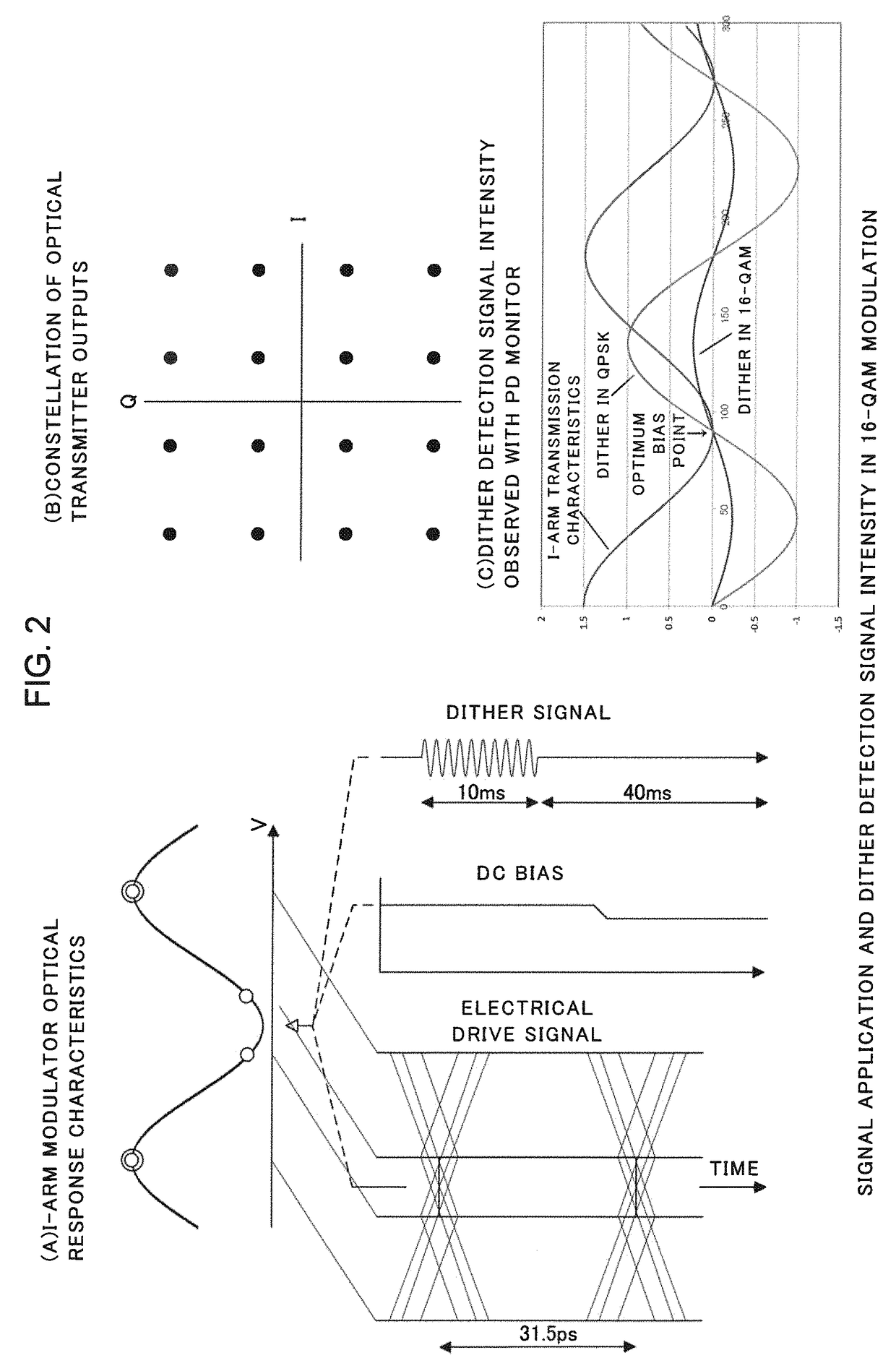
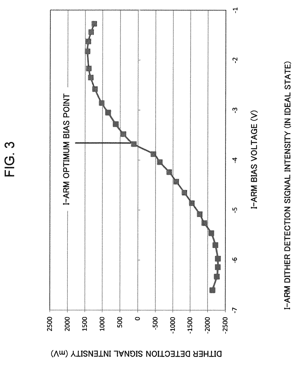
[0106]A first example embodiment is based on a finding (results of experiments by the present inventors) that since a noise component produced by I / Q quadrature skew is mixed in bias control for an I-arm or Q-arm in an optical transmitter that includes a multilevel modulation unit such as a 16-QAM modulation unit, the stability of the I-arm or the Q-arm control can be increased by observing I / Q quadrature skew concurrently and removing the noise component from a bias control signal for the I-arm or the Q-arm.

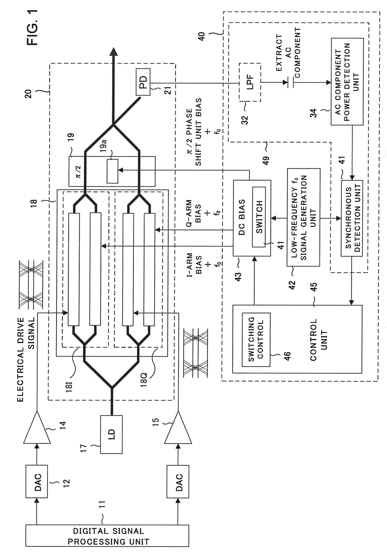
[0107]FIG. 6 is a diagram illustrating a configuration of an optical transmitter 129 of a first example embodiment. In the first example embodiment, 16-QAM modulation is applied to an optical modulator (IQ modulator) 105 and a portion of its output light is extracted as a monitor signal. A control signal is generated from the monitor signal to control biases of an I-arm and a Q-arm and a bias of an optical π / 2 phase shift unit 108.

[0108]The optical transmitter 129 includes a las...

second example embodiment

[0208]FIG. 14 is a diagram illustrating a configuration of an optical transmitter according to a second example embodiment. Differences form the first example embodiment in FIG. 6 are:[0209]a method of superimposing a dither signal on an optical π / 2 phase shift unit 108,[0210]a method of acquiring a control signal for I / Q quadrature control, and[0211]an ABC control circuit schedule.

[0212]I / Q quadrature control operation is performed along with bias control for an I-arm modulator and a Q-arm modulator, thereby reducing control sequence time and start-up time of an optical transmitter 144, and stabilizing an ABC circuit.

[0213]In FIG. 14, a dither signal cut from a signal from a low-frequency oscillator 117 is not superimposed on a bias signal 126 (bias signal 126 to an optical π / 2 phase shift unit 108) output from a DC bias generation unit 122 in a control unit 142.

[0214]The dither signal is superimposed on a bias signal 124 for an I-arm modulator 106 and a bias signal 125 for a Q-arm...

third example embodiment

[0225]FIG. 16 is a diagram illustrating a configuration of an optical transmitter of a third example embodiment. The third example embodiment differs from the first example embodiment in FIG. 6 in that in place of the noise remover 120, a control value selector 151 is provided in a control unit 153 to simplify the control process of the control unit 153, thereby providing an ABC circuit 154 aimed to achieve stable operation.

[0226]In the third example embodiment in FIG. 16, an RMS detection value 115 from a signal amplitude detector 114 is selected and output as a noise component 131, which is one of outputs of a noise component detector 119 in the control unit 153. For the control value selector 151 into which the noise component 131 is input, a threshold input unit 152 is provided as another input signal source.

[0227]On the other hand, as a control signal 132, which is another output of the noise component detector 119, an envelope detection signal 116 from the signal amplitude det...


PUM

PropertyMeasurementUnit
quadrature angleaaaaaaaaaa
I/Q quadrature angleaaaaaaaaaa

Abstract

To provide a modulation control method and an optical transmission device that realize high reliability by more stably performing bias control of an optical modulator using an optical QAM scheme, an optical transmitter according to the present invention comprises a first waveguide and a second waveguide, wherein each of the first waveguide and the second waveguide are provided with an optical modulator that modulates a carrier light with a modulation driving signal that has multiple strength level values, a phase shift unit that provides a predetermined phase difference between a first optical signal outputted from the first waveguide and a second optical signal outputted from the second waveguide, a light detector that detects and photoelectrically converts a portion of a multiple value optical signal obtained by multiplexing the first optical signal and the second optical signal which have been provided with the phase difference and a control circuit that, on the basis of signal amplitude information obtained by a signal amplitude detector from wideband signal components from the light detector, corrects a first voltage provided to the first waveguide and corrects a second voltage provided to the second waveguide.

Description

[0001]This application is a National Stage Entry of PCT / JP2016 / 001585 filed on Mar. 18, 2016, which claims priority from Japanese Patent Application 2015-063960 filed on Mar. 26, 2015, the contents of all of which are incorporated herein by reference, in their entirety.TECHNICAL FIELD[0002]The present invention relates to an optical transmission device and a method of controlling the optical transmission device.BACKGROUND ART[0003]One way to optimize investment in optical fiber communications in order to cope with increase in information transmission demand in optical fiber communications is to employ a more efficient modulation scheme for transmitted information to increase the spectral efficiency.[0004]To meet this direction, modulation schemes based on Quadrature Phase Shift Keying (QPSK), for example, have been developed for optical communication systems having larger capacities. In this case, information is encoded into four phase levels. Accordingly, 2 bits of binary signal pe...

Claims


Application Information

Patent Timeline
Patent Type & Authority Patents(United States)
IPC IPC(8): G02F1/01H04B10/516G02F1/225H04B10/556G02F1/21
CPCG02F1/0123G02F1/225H04B10/5561H04B10/516G02F2201/58G02F2001/212G02F1/212H04B10/50575H04B10/541
Inventor FUJITA, SADAOLE TAILLANDIER DE GABORY, EMMANUEL
Owner NEC CORP
Why Eureka
Try Eureka