MicroLED display panel

a display panel and micro-lead technology, applied in the field of display panels, can solve the problems of thermal mismatch, significantly affected, and more complex than flip chip technology, and achieve the effects of reducing the loading of drivers, simplifying the process of making display panels, and reducing the turn-on time of micro-leads

Active Publication Date: 2019-02-05
PRILIT OPTRONICS INC
View PDF4 Cites 2 Cited by
  • Summary
  • Abstract
  • Description
  • Claims
  • Application Information

AI Technical Summary

Benefits of technology

The present invention provides a microLED display panel that can reduce the burden on drivers and make it feasible to create large-size, high-resolution displays. The passive driving scheme simplifies the manufacturing process, reduces the turn-on time of the microLEDs, increases the drive current, and effectively minimizes the impact on gray display due to leakage current.

Problems solved by technology

However, microLED is made by flip chip technology, while TFT is made by complementary metal-oxide-semiconductor (CMOS) process which is more complex than flip chip technology.
These two distinct technologies may cause thermal mismatch.
A drive current of the microLED is small in gray display, which may be significantly affected by leakage current.
When the size or the resolution of the display panel increases, output loading and delay of the drive circuits increase accordingly, causing the display panel to malfunction.
Therefore, passive matrix is not suitable for large-size microLED display panels.

Method used


Image

  • MicroLED display panel
  • MicroLED display panel
  • MicroLED display panel

Examples


first embodiment

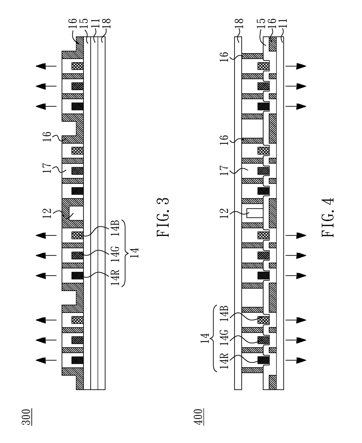
[0032]FIG. 6A shows a partial enlarged side view of a microLED display panel according to the present invention. In the embodiment, a top surface of the substrate 11 has a recess 110 for accommodating an integrated circuit (e.g., the driver 12). In the embodiment, a sum of a depth d1 of the recess 110 and a height of the microLED 14 is substantially equal to a height of the driver 12. Accordingly, a top surface of the driver 12 and the top surface of the microLED 14 are at a substantially same level. Compared with the microLED display panel shown in FIG. 5, light emitted from the microLEDs 14 of the embodiment is not blocked by the neighboring driver 12.

second embodiment

[0033]FIG. 6B shows a partial enlarged side view of a microLED display panel according to the present invention. In the embodiment, a top surface of the substrate 11 has a recess 110 for accommodating an integrated circuit (e.g., the driver 12). In the embodiment, a depth d2 of the recess 110 is greater than a height of the driver 12. Accordingly, a top surface of the driver 12 is at a level lower than a top surface of the microLED 14. Compared with the microLED display panel shown in FIG. 5, light emitted from the microLEDs 14 of the embodiment is not blocked by the neighboring driver 12.

third embodiment

[0034]FIG. 6C shows a partial enlarged side view of a microLED display panel according to the present invention. In the embodiment, a top surface of the substrate 11 has a recess 110 for accommodating an integrated circuit (e.g., the driver 12). In the embodiment, a sum of a depth d3 of the recess 110 and a height of the microLED 14 is less than a height of the driver 12. Accordingly, a top surface of the driver 12 is at a level higher than a top surface of the microLED 14. Compared with the microLED display panel shown in FIG. 5, substantially less light emitted from the microLEDs 14 of the embodiment is blocked by the neighboring driver 12.

[0035]According to the embodiments discussed above, one may design recesses with different depths for accommodating integrated circuits with different heights according to the heights of the integrated circuits, respectively. One may design a groove with plural recesses according to the integrated circuit with the maximum height for accommodatin...


PUM


Abstract

A microLED display panel includes a substrate being divided into a plurality of sub-regions for supporting microLEDs, and a plurality of drivers being correspondingly disposed on surfaces of the sub-regions respectively. In one embodiment, a top surface of the substrate has a recess for accommodating the driver.

Description

BACKGROUND OF THE INVENTION1. FIELD OF THE INVENTION[0001]The present invention generally relates to a display panel, and more particularly to a microLED display panel.2. DESCRIPTION OF RELATED ART[0002]A micro light-emitting diode (microLED, mLED or μLED) display panel is one of flat display panels, which is composed of microscopic microLEDs each of a size of 1-10 micrometers. Compared to conventional liquid crystal display panels, the microLED display panels offer better contrast, response times and energy efficiency. Although both organic light-emitting diodes (OLEDs) and microLEDs possess good energy efficiency, the microLEDs, based on group III / V (e.g., GaN) LED technology, offer higher brightness, higher luminous efficacy and longer lifespan than the OLEDs.[0003]Active matrix using thin-film transistors (TFT) may be used in companion with microLEDs to drive a display panel. However, microLED is made by flip chip technology, while TFT is made by complementary metal-oxide-semico...

Claims


Application Information

Patent Timeline
Patent Type & Authority Patents(United States)
IPC IPC(8): H01L29/18H01L25/16H01L33/56H01L33/54H01L25/075
CPCH01L25/167H01L33/56H01L33/54H01L25/0753H01L33/46
Inventor WU, BIING-SENGWU, CHAO-WEN
Owner PRILIT OPTRONICS INC
Why Eureka
Try Eureka