Organic electroluminescent display panel and display apparatus

a technology of electroluminescent display panel and display apparatus, which is applied in the field of display technology, can solve the problems of generating a larger voltage drop, adversely affecting the light emitting efficiency of the oled, and damage to the oled device, so as to reduce the resistance of the cathode, avoid damage to the organic electroluminescent, and increase the equivalent thickness of the cathode

Active Publication Date: 2019-02-12
BOE TECH GRP CO LTD
View PDF20 Cites 3 Cited by
  • Summary
  • Abstract
  • Description
  • Claims
  • Application Information

AI Technical Summary

Benefits of technology

[0011]In the above organic electroluminescent display panel provided by embodiments of the present invention, because the secondary electrode is additionally provided on the packaging film and is electrically connected with the cathode through the via hole penetrating through the packaging film, the secondary electrode electrically connected with the cathode can increase an equivalent thickness of the cathode and thus reduce the resistance of the cathode, which can avoid the problem of large voltage drop due to the large resistance of the cathode when a thinner metal is used as the cathode, thereby can avoid damage of the organic electroluminescent display panel due to large voltage drop.

Problems solved by technology

The light emitting layer below the cathode, however, will be damaged when manufacturing the cathode by using the magnetron sputtering process, thereby adversely affecting light emitting efficiency of the OLED.
The formed thin layer of metal has a larger resistance, and especially when being applied in an OLED device of larger size, will generate a larger voltage drop and damage the OLED device.
Thus, a technical problem to be solved in the art is how to avoid the problem of large voltage drop due to the large resistance of the cathode.

Method used


Image

  • Organic electroluminescent display panel and display apparatus
  • Organic electroluminescent display panel and display apparatus
  • Organic electroluminescent display panel and display apparatus

Examples


Embodiment Construction

[0027]Specific embodiments of the organic electroluminescent display panel and the display apparatus according to the present invention will be described hereinafter in detail in conjunction with the attached drawings.

[0028]Shapes and thicknesses of respective film layers shown in the drawings are not scaled to the real proportion, and positional relationships of the respective film layers may be varied and some film layers may be omitted. Thus, the drawings are intended to only illustrate exemplary embodiments of the present invention, but not to limit the present invention.

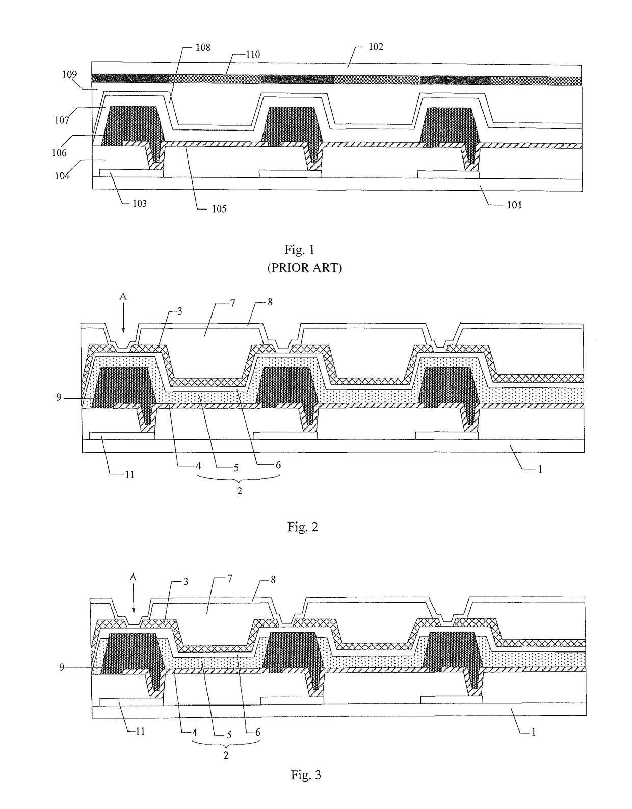
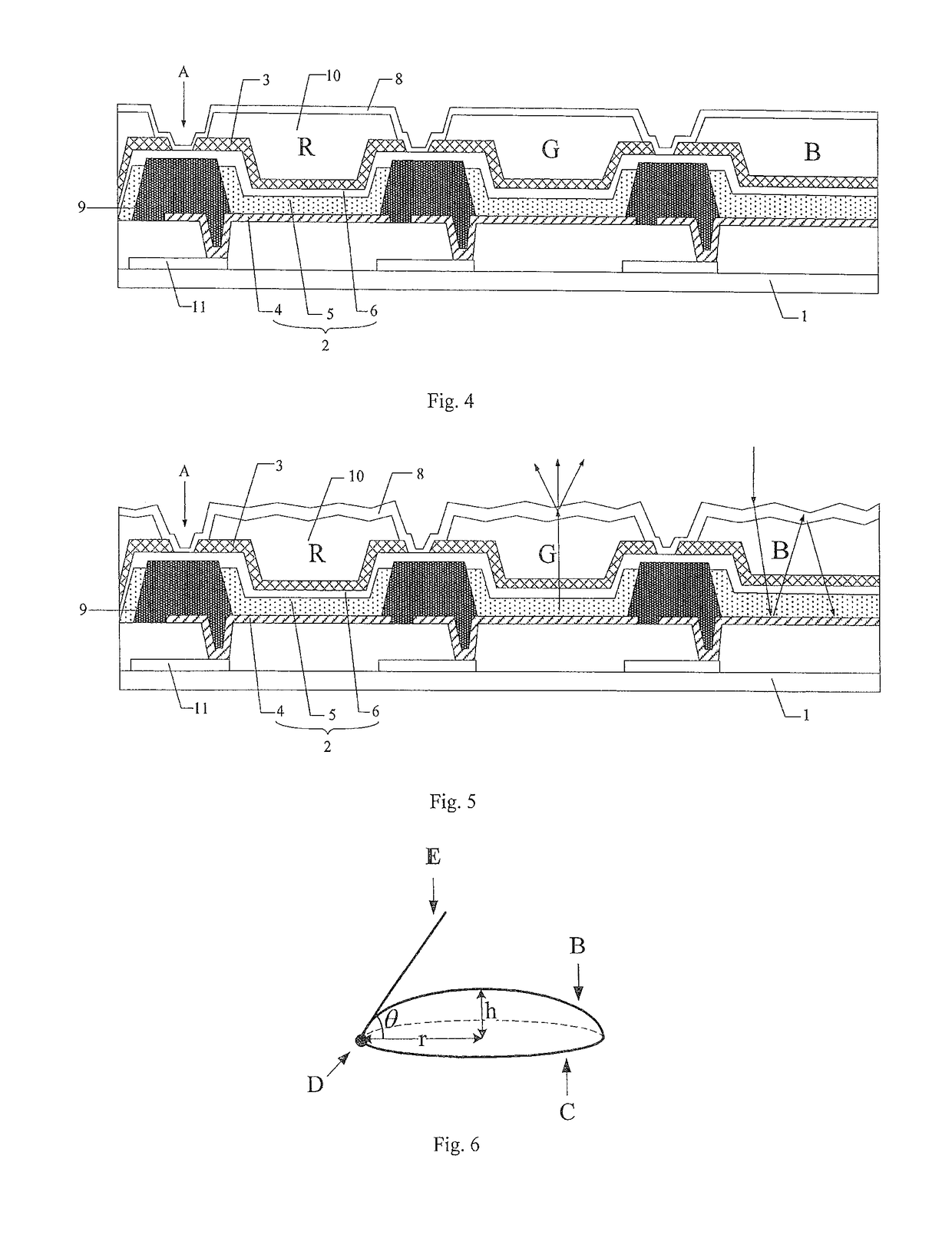
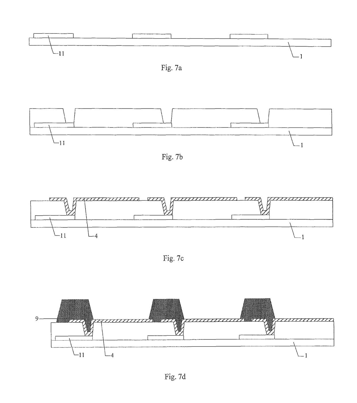
[0029]FIG. 2 schematically shows a structure of an organic electroluminescent display panel according to one embodiment of the present invention. As shown in FIG. 2, the organic electroluminescent display panel comprises: a base substrate 1, a top-emitting type organic electroluminescent structure 2 located on the base substrate 1, and a packaging film 3 covering the organic electroluminescent structure 2. The o...


PUM


Abstract

The present invention discloses an organic electroluminescent display panel, comprising: a base substrate; a top-emitting type organic electroluminescent structure located on the base substrate, the organic electroluminescent structure comprising an anode, a light emitting layer and a cathode arranged in this order from the base substrate; and a packaging film covering the organic electroluminescent structure; the organic electroluminescent display panel further comprises a secondary electrode provided on the packaging film and electrically connected with the cathode through a via hole penetrating through the packaging film. Since the secondary electrode is additionally provided on the packaging film and is electrically connected with the cathode through the via hole penetrating through the packaging film, the secondary electrode electrically connected with the cathode can increase an equivalent thickness of the cathode and thus reduce the resistance of the cathode, which can avoid the problem of large voltage drop due to large resistance of the cathode when a thinner metal is used as the cathode, thereby can avoid damage of the organic electroluminescent display panel due to the larger voltage drop.

Description

CROSS-REFERENCE TO RELATED APPLICATION[0001]This application is a Section 371 National Stage application of International Application No. PCT / CN2014 / 089161, filed Oct. 22, 2014, which has not yet published, which claims priority to Chinese Patent Application No. 201410240373.6, filed May 30, 2014, in Chinese, the contents of which are hereby incorporated by reference in their entirety.BACKGROUND OF THE INVENTION[0002]Field of the Invention[0003]The present invention relates to the field of display technology, and particularly, to an organic electroluminescent display panel and display apparatus.[0004]Description of the Related Art[0005]An organic electroluminescent display (OLED) device, among existing flat panel display devices, has been widely used in the field of display due to its characteristics such as low power consumption, high color saturation, wide angle of view and the like.[0006]The OLED devices can be classified into a top-emitting type OLED device and a bottom-emitting...

Claims


Application Information

Patent Timeline
Patent Type & Authority Patents(United States)
IPC IPC(8): H01L51/52H01L27/32
CPCH01L51/5253H01L27/322H01L51/5221H01L27/3246H01L27/3279H01L27/3211H10K59/35H10K59/38H10K59/1315H10K59/873H10K59/8052H10K50/844H10K50/82H10K59/122
Inventor SONG, YOUNG SUKYOO, SEONG YEOLCHOI, SEUNG JINKIM, HEE CHEOL
Owner BOE TECH GRP CO LTD
Why Eureka
Try Eureka