Antenna device and communication terminal device

a technology of communication terminal and antenna device, which is applied in the direction of resonant antenna, loop antenna with ferromagnetic core, differential interacting antenna combinations, etc., can solve the problems of increasing the number of manufacturing processes, the need to consider the mechanical strength decrease, and the inability of the antenna to communicate with the party-side antenna, so as to prevent the reduction of an electric field shielding effect and the mechanical strength. effect of strength

Active Publication Date: 2019-03-05
MURATA MFG CO LTD
View PDF16 Cites 0 Cited by
  • Summary
  • Abstract
  • Description
  • Claims
  • Application Information

AI Technical Summary

Benefits of technology

[0009]Preferred embodiments of the present invention provide an antenna device that prevents problems of a decrease in mechanical strength, design restrictions, and a decrease in electric field shielding effect, and that also significantly reduces or prevents the problem of interference with another high-frequency circuit, if necessary, by enabling a conductor surface defined by a metal plate or the like to be used as a radiation element without a slit or an opening provided in the metal plate, and also provide a communication terminal device including the antenna device.
[0018]Various preferred embodiments of the present invention enables the two conductor surfaces to be used as radiation elements without providing a slit or an opening in a conductor surface. Therefore, problems of a decrease in mechanical strength, design restriction, and a decrease in an electric field shielding effect are prevented.

Problems solved by technology

Due to the shielding of the electromagnetic field, there arises a problem that the antenna cannot make communication with a party-side antenna.
However, with provision of a slit or an opening in the metal plate, a decrease in the mechanical strength needs to be considered, and the number of processes in manufacturing increases.
Further, when a slit or an opening is to be provided in a metal housing, in particular, design of the housing is restricted.
In addition, the vicinity of the slit or the opening cannot be connected to the ground of a circuit.
Therefore, the potential of the metal plate partially fluctuates in some cases, resulting in a problem that an electric field shielding effect of the metal plate decreases or a concern over interference of a first conductor surface and a second conductor surface with another high-frequency circuit is generated.

Method used


Image

  • Antenna device and communication terminal device
  • Antenna device and communication terminal device
  • Antenna device and communication terminal device

Examples


first preferred embodiment

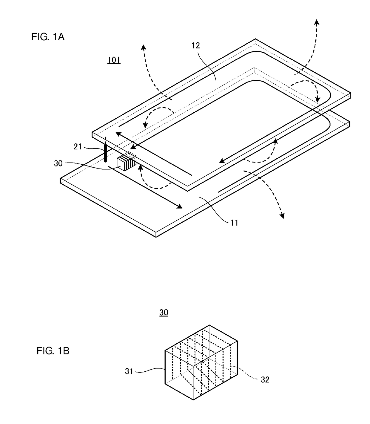
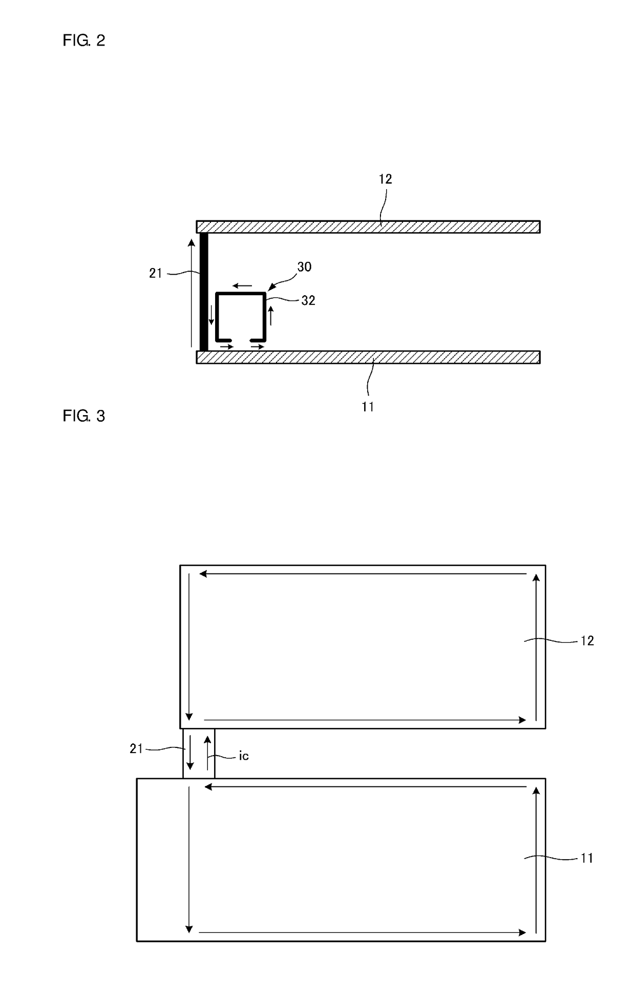
[0027]FIG. 1A is a perspective view of an antenna device 101 according to a first preferred embodiment of the present invention, and FIG. 1B is a perspective view of an antenna coil 30 provided in the antenna device 101. FIG. 2 is a front view of the antenna device 101. The antenna device 101 preferably is an antenna that is used in an HF band of 13.56 MHz or the like, for example, and generates proximity-type or vicinity-type electromagnetic field coupling (magnetic field coupling, mainly) with an antenna of a communication party.

[0028]The antenna device 101 includes a first conductor surface 11 and a second conductor surface 12 opposing each other. The first conductor surface 11 and the second conductor surface 12 are connected with each other with a first connection conductor 21 (referred to as a “first” connection conductor in order to distinguish it from a second connection conductor, which will be described in another preferred embodiment later). The antenna coil 30 is arrange...

second preferred embodiment

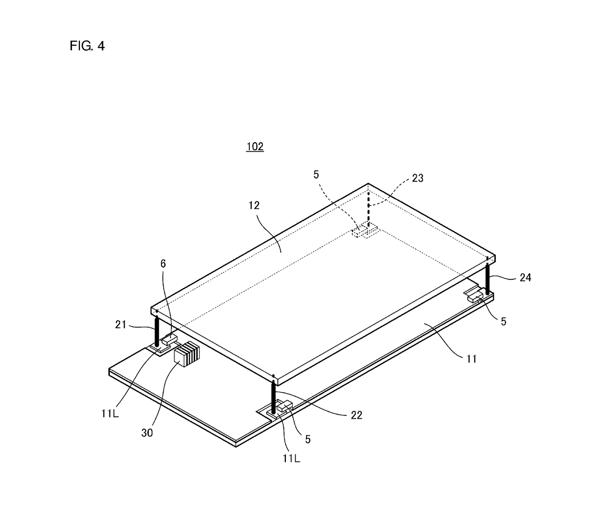
[0036]FIG. 4 is a perspective view of an antenna device 102 according to a second preferred embodiment of the present invention. The antenna device 102 includes the first connection conductor 21 and a plurality of second connection conductors 22, 23, and 24. These connection conductors 21 to 24 are located at the edges of the first conductor surface 11 and the second conductor surface 12. The first connection conductor 21 allows a land 11L and the second conductor surface 12 to become conductive. A chip inductor 6 is mounted between the land 11L and the first conductor surface 11. That is to say, the first conductor surface 11 and the second conductor surface 12 are connected with each other with the chip inductor 6 interposed therebetween at a portion around the first connection conductor 21.

[0037]The second connection conductor 22 allows a land 11L and the second conductor surface 12 to become conductive. A chip capacitor 5 is mounted between the land 11L and the first conductor s...

third preferred embodiment

[0040]FIG. 5 is a plan view illustrating a configuration of an inner portion of a communication terminal device according to a third preferred embodiment of the present invention. Circuit substrates 61 and 62, a battery pack 90, a camera module 76, and so on are accommodated in an upper housing 91. An RFIC 60 including a communication circuit, a resonance capacitor C, the antenna coil 30, and so on are mounted on the circuit substrate 61. A main UHF-band antenna 82 and so on are also provided on the circuit substrate 61. Further, a sub UHF-band antenna 83 and so one are provided on the circuit substrate 62. A circuit on the circuit substrate 61 and a circuit on the circuit substrate 62 are connected with each other with a cable interposed therebetween. The UHF-band antennas 82 and 83 are provided by mounting chip antennas, forming line patterns, or the like.

[0041]A ground electrode is provided on substantially an overall area of the circuit substrate 61, and the ground electrode def...


PUM


Abstract

An antenna device includes two conductor surfaces at opposing positions with a space interposed between the conductor surfaces, a first connection conductor connecting the two conductor surfaces galvanically at one location, and an antenna coil arranged in proximity to the first connection conductor. The antenna coil is arranged at a position at which the antenna coil causes an induced current to flow through the first connection conductor by electromagnetic induction. Currents in the opposite directions flow through peripheral edge portions of the two conductor surfaces, so that a magnetic field is radiated from A space across which the two conductor surfaces oppose each other. This enables a conductor surface defined by a metal plate or the like to be used as a radiation element without providing a slit or an opening in the metal plate so as to avoid problems of a decrease in mechanical strength, design restrictions, and a decrease in an electric field shielding effect.

Description

BACKGROUND OF THE INVENTION[0001]1. Field of the Invention[0002]The present invention relates to an antenna device and a communication terminal device that are preferably used for a communication system using a high-frequency (HF) band or an ultra-high-frequency (UHF) band.[0003]2. Description of the Related Art[0004]In a device that is included in an electronic apparatus, such as a cellular phone, and performs HF-band communication, such as a near field communication (NFC), a radio-frequency integrated circuit (RFIC) and a matching element are typically mounted on a circuit substrate, an antenna is bonded to the inner side of a housing of the electronic apparatus, and the RFIC and the antenna are electrically connected to each other with a spring pin or the like interposed therebetween.[0005]Meanwhile, a reduction in the thickness of a recent wireless communication terminal such as the cellular phone terminal has advanced, and “metallization” by applying magnesium plating to a hous...

Claims


Application Information

Patent Timeline
Patent Type & Authority Patents(United States)
IPC IPC(8): H01Q1/24H01Q9/04H01Q1/50H01Q1/48H01Q7/00H01Q21/29H01Q7/08H01Q1/22
CPCH01Q1/243H01Q1/22H01Q1/48H01Q21/29H01Q7/00H01Q7/08H01Q9/0407H01Q1/50
Inventor KATO, NOBORU
Owner MURATA MFG CO LTD
Why Eureka
Try Eureka