Semiconductor device, liquid discharge head, liquid discharge head cartridge, and printing apparatus

a technology of liquid discharge head and liquid discharge head, which is applied in the direction of semiconductor devices, printing, basic electric elements, etc., can solve the problems of difficult to reduce the voltage applied to the discharge elements by the wiring pattern, and achieve the effect of reducing the restriction on the layout, and reducing the voltage variation

Active Publication Date: 2019-04-16
CANON KK
View PDF18 Cites 0 Cited by
  • Summary
  • Abstract
  • Description
  • Claims
  • Application Information

AI Technical Summary

Benefits of technology

[0003]In some cases, it may be difficult to reduce the variation in the voltage applied to the discharge elements by the wiring pattern because there is a restriction on the layout to, for example, arrange the terminal unit for the power supply wiring line and the ground wiring line on one side. An aspect of the present invention provides a technique advantageous in reducing a restriction on the layout of wiring lines and a terminal unit while reducing a variation in a voltage applied to discharge elements.
[0006]According to some other embodiments, a liquid discharge head comprises a discharge portion configured to discharge a liquid and a semiconductor device arranged to control the discharge of the liquid from the discharge portion, the semiconductor device comprising a plurality of discharge units each including a discharge element configured to discharge a liquid, and a driving unit configured to drive the discharge element; and a terminal unit configured to supply power to each of the plurality of discharge units via a wiring line, wherein the plurality of discharge units includes a first discharge unit and a second discharge unit, the first discharge unit includes a first discharge element of the discharge elements and a first driving unit of the driving units, the second discharge unit includes a second discharge element of the discharge elements and a second driving unit of the driving units, a length of a current path from the terminal unit to the first discharge unit is longer than a length of a current path from the terminal unit to the second discharge unit, and a resistance of the first driving unit is lower than a resistance of the second driving unit.

Problems solved by technology

In some cases, it may be difficult to reduce the variation in the voltage applied to the discharge elements by the wiring pattern because there is a restriction on the layout to, for example, arrange the terminal unit for the power supply wiring line and the ground wiring line on one side.

Method used


Image

  • Semiconductor device, liquid discharge head, liquid discharge head cartridge, and printing apparatus
  • Semiconductor device, liquid discharge head, liquid discharge head cartridge, and printing apparatus
  • Semiconductor device, liquid discharge head, liquid discharge head cartridge, and printing apparatus

Examples


first embodiment

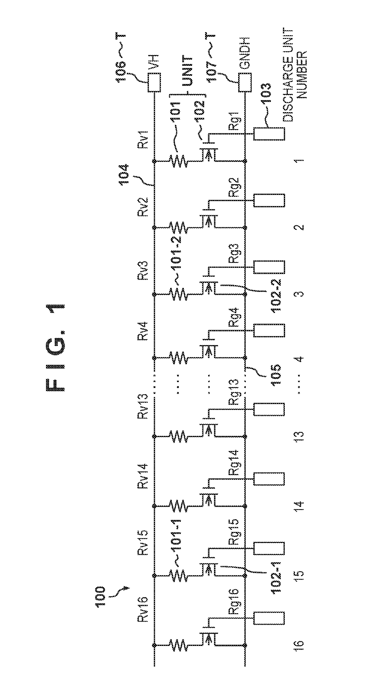
[0027]The structure of a semiconductor device according to an embodiment of the present invention will be described with reference to FIGS. 1 to 4. FIG. 1 is a circuit diagram showing the circuit arrangement of a semiconductor device 100 according to the present invention. The semiconductor device 100 is configured to control discharge of a liquid. The semiconductor device 100 is configured to control discharge of a liquid from a discharge portion in, for example, a printing apparatus that prints an image on a printing medium such as paper using a liquid such as ink.

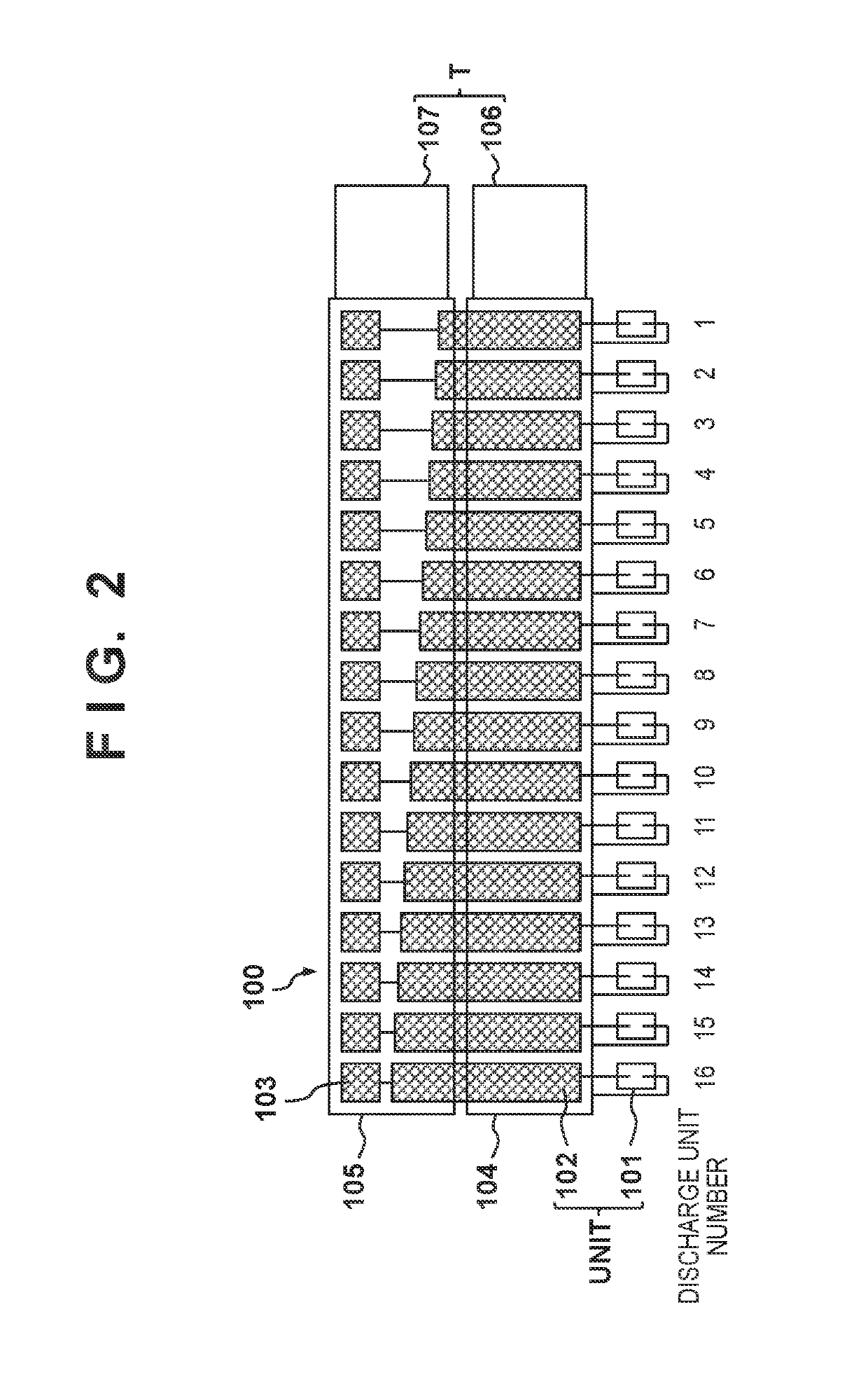
[0028]The semiconductor device 100 includes a terminal unit T including a power supply terminal 106 (VH terminal) and a ground terminal 107 (GNDH terminal), a plurality of discharge units UNIT, a power supply wiring line 104 (VH wiring line), and a ground wiring line 105 (GNDH wiring line). The power supply terminal 106 and the ground terminal 107 supply power to the discharge units UNIT via the power supply wiring line ...

third embodiment

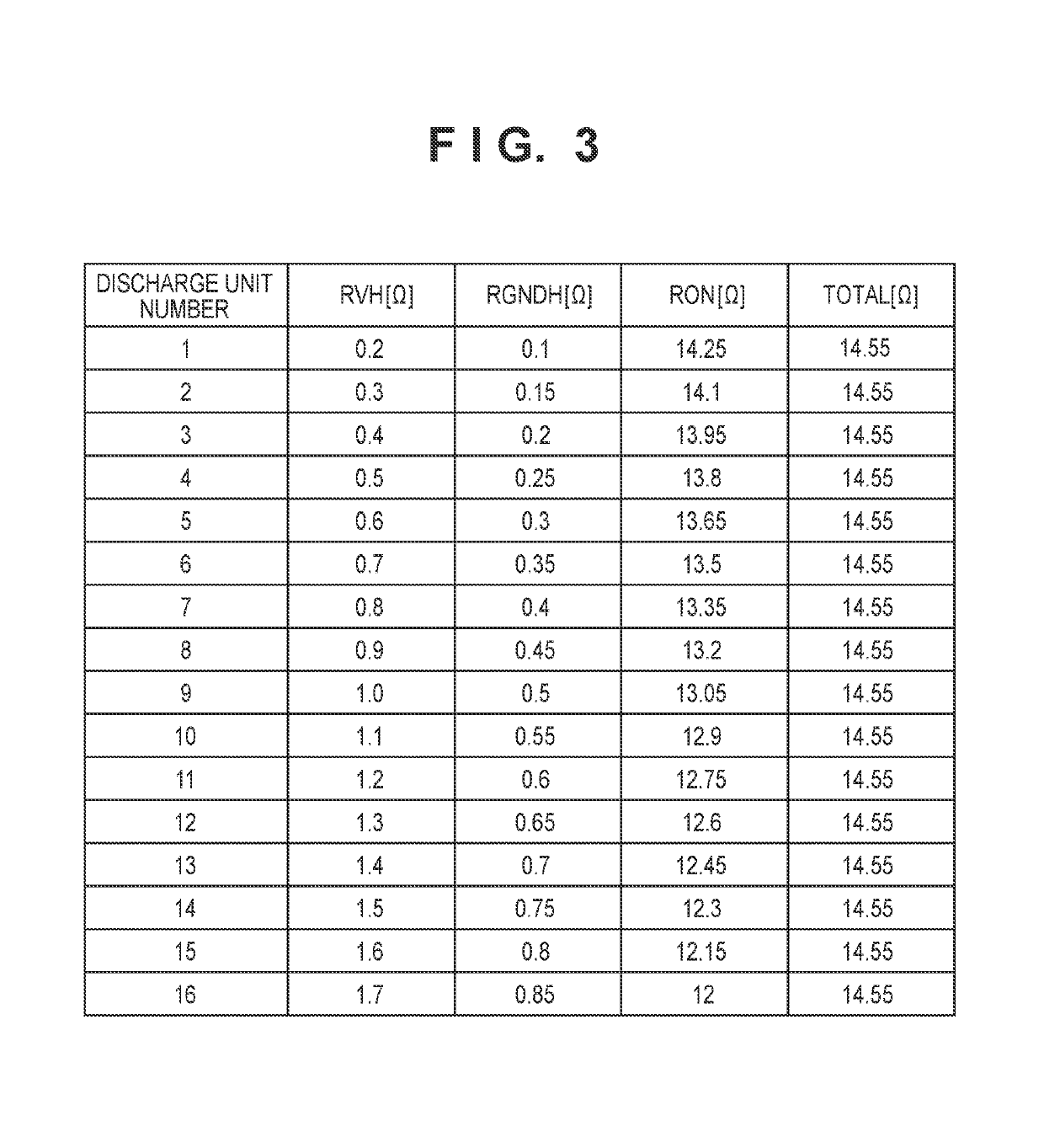
[0080]The drivability of the transistors of the driving units 102 is changed not only in the column direction 311 but also in the row direction 312. With this arrangement, the difference between the maximum value and the minimum value of the total resistance value of the wiring resistance RVH of the power supply wiring line 104, the wiring resistance RGNDH of the ground wiring line 105, and the ON resistance RON of the transistors of the driving units 102 can be reduced to 0.14 Ω, as shown in FIG. 15. When the arrangement according to this embodiment is used, the variation in the sum of the wiring resistances and the ON resistance of the transistors inserted in the current path of each discharge unit UNIT between the power supply terminal 106 and the ground terminal 107 can further be reduced as compared to the above-described It is therefore possible to reduce the variation in the voltage applied to the discharge elements 101 and further improve the image quality of a formed image...


PUM


Abstract

A semiconductor device is provided. The device comprises discharge units each including a discharge element and a driving unit configured to drive the discharge element, and a terminal unit configured to supply power to the discharge units via a wiring line. The discharge units include a first discharge unit including a first discharge element of the discharge elements and a first driving unit of the driving units and a second discharge unit including a second discharge element of the discharge elements and a second driving unit of the driving units. A length of a current path from the terminal unit to the first discharge unit is longer than a length of a current path from the terminal unit to the second discharge unit and a resistance of the first driving unit is lower than a resistance of the second driving unit.

Description

BACKGROUND OF THE INVENTIONField of the Invention[0001]The present invention relates to a semiconductor device, a liquid discharge head, a liquid discharge head cartridge, and a printing apparatus.Description of the Related Art[0002]There is known a liquid discharge head that gives an energy generated by a discharge element to a liquid, thereby discharging the liquid from a discharge portion. To implement high-speed printing, a plurality of discharge elements is arranged in the liquid discharge head. If the voltage applied to the discharge elements varies, the amount of the discharge liquid varies, and the image quality of a formed image may lower. Japanese Patent Laid-Open No. 2014-94514 discloses a wiring pattern configured to reduce a variation in the voltage applied to the discharge elements, which is caused by a wiring resistance that changes in accordance with the wiring length from a terminal unit to each discharge element, when supplying power to the plurality of discharge e...

Claims


Application Information

Patent Timeline
Patent Type & Authority Patents(United States)
IPC IPC(8): B41J2/045H01L27/088H01L23/528H01L27/092
CPCB41J2/04541B41J2/0458B41J2/04548B41J2/04581H01L27/088B41J2/04586H01L27/0922H01L23/528H01L27/092
Inventor TAKAGI, MAKOTO
Owner CANON KK
Why Eureka
Try Eureka