Electronically functional yarns

a technology of functional yarns and electrons, applied in the field of yarns, can solve the problems of compromising the surface of yarn, not providing a resolution, and avoiding the risk of such exposure, and achieve the effects of extending the length of the yarn, avoiding the risk of such exposure, and enhancing the efficiency of the devi

Active Publication Date: 2019-05-28
NOTTINGHAM TRENT UNIVERSITY
View PDF16 Cites 7 Cited by
  • Summary
  • Abstract
  • Description
  • Claims
  • Application Information

AI Technical Summary

Benefits of technology

[0007]A primary aim of the present invention is to avoid risk of such exposure and thereby enhance the efficiency of a device in a series of devices installed in a yarn. Another aim is to incorporate devices and connections thereto in a yarn in such a manner that they are unobtrusive. According to the invention an electronically functional yarn comprises a plurality of carrier fibres forming a core; a series of electronic devices mounted on the core with conductive interconnects extending along the core; a plurality of packing fibres around the core, the devices and the interconnects; and a retaining sleeve around the packing fibres, wherein the core, the devices and the interconnects are confined within the plurality of packing fibres retained in the sleeve. The interconnects can comprise at least one conductor that extends the length of the yarn. By mounting the devices and interconnects on carrier fibres they are more easily retained in the bod

Problems solved by technology

However, where the device has an electrical connection the connection will be exposed on the yarn surface and thereby compromised by contact with other

Method used


Image

  • Electronically functional yarns
  • Electronically functional yarns
  • Electronically functional yarns

Examples


Embodiment Construction

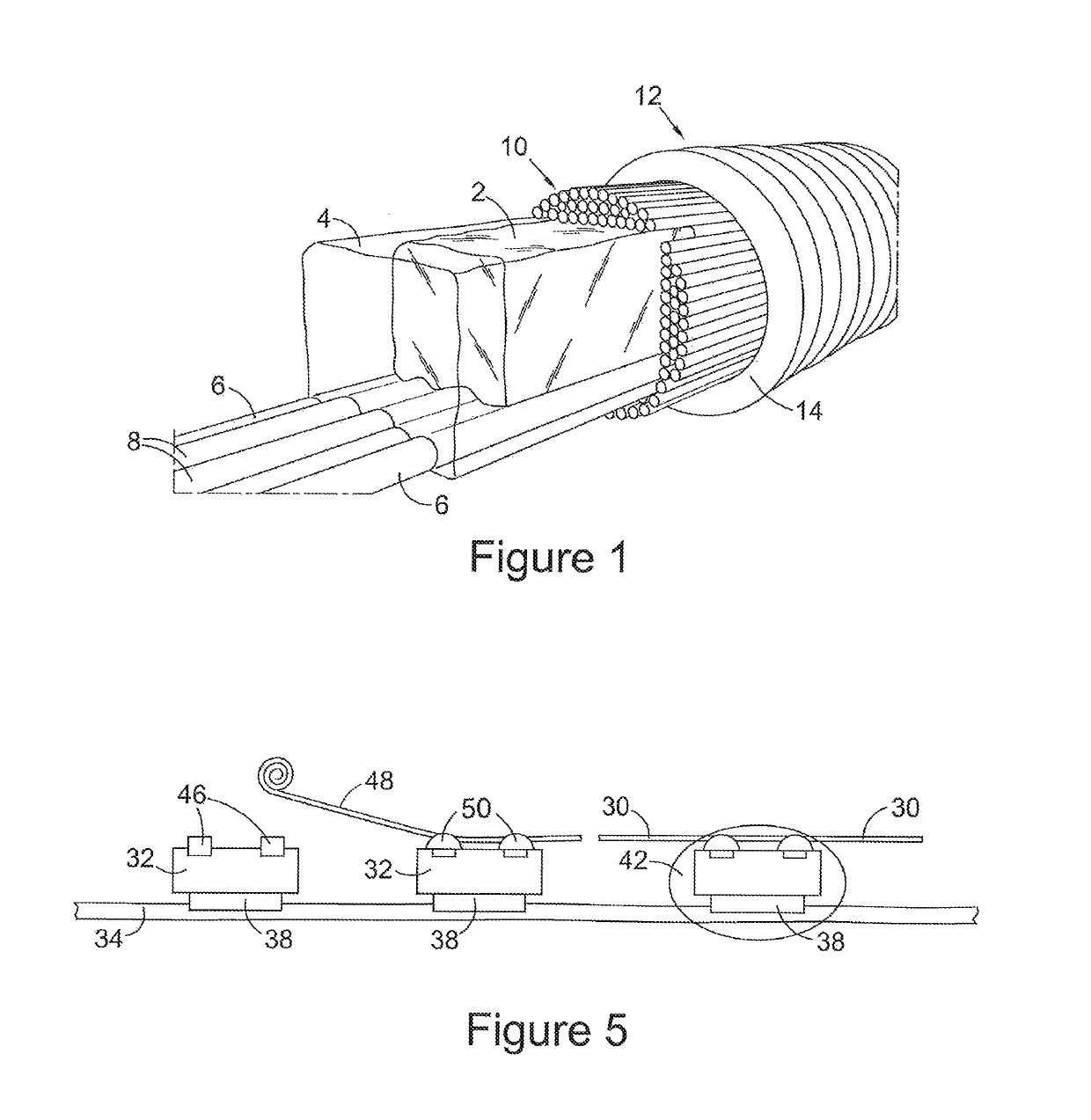
[0020]In the yarn shown in FIG. 1 a semiconductor chip 2 is sealed in a polymeric micro-pod 4 which extends around four 100 μm PBI carrier fibres 6. The chip shown is 900 μm long and has a square cross section of 500×500 μm. Two 150 μm copper filament interconnects 8 extend from the chip 2 within the pod 4 over the carrier fibres 6. Polyester packing fibres 10 (diameter 10 μm) extend around the pod 4, the carrier fibres 6, and the interconnects 8. As shown they extend substantially parallel to the yarn axis, but may be bunched or twisted to fill the spaces between the pods 4. A filler (not shown) may also be used for this purpose. Some twisting of the packing fibres around the pods 4 can also be of value to provide a protective layer, but this will depend upon the shape of the pod. The linear arrangement of packing fibres shown can be more appropriate when the pod 4 is rectanguloid or cylindrical in shape. Whatever arrangement is selected some of the packing fibres 10 can be bonded ...


PUM

PropertyMeasurementUnit
Lengthaaaaaaaaaa

Abstract

An electronically functional yarn comprises a plurality of carrier fibers (6) forming a core with a series of electronic devices (2) mounted on the core with conductive interconnects (8) extending along the core. A plurality of packing fibers (10) are disposed around the core, the devices and the interconnects, and a retaining sleeve (12) is disposed around the packing fibers. The core, the devices and the interconnects are confined within the plurality of packing fibers retained in the sleeve. In the manufacture of the yarn the electronic devices with interconnects coupled thereto in sequence are mounted on the core; the carrier fibers with the mounted devices and interconnects are fed centrally through a channel with packing fibers around the sides thereof to form a fiber assembly around the core, which is fed into a sleeve forming unit in which a sleeve is formed around the assembly to form the composite yarn.

Description

CROSS-REFERENCED TO RELATED APPLICATIONS[0001]This application claims priority from Application PCT / GB2015 / 052553, filed Sep. 4, 2015, which is deemed incorporated by reference in its entirety in this application.STATEMENT REGARDING FEDERALLY SPONSORED RESEARCH OR DEVELOPMENT[0002]Not applicable.BACKGROUND OF THE INVENTIONI. Field of the Invention[0003]This invention relates to yarns incorporating electronic devices and their manufacture. It relates particularly to such yarns in which the devices and electrical connections thereto are protected. Also part of the invention is a method of manufacturing the yarns for incorporation into fabric products for example, although other uses are contemplated.II. Discussion of the Prior Art[0004]International Patent Publication No. WO2006 / 123133, the contents whereof are hereby incorporated by reference, discloses a multi-filament yarn including an operative devices confined between the yarn filaments, and a method for its manufacture. The yarn...

Claims


Application Information

Patent Timeline
IPC IPC(8): D02G3/02D02G3/22D02G3/44D02G3/36
CPCD02G3/36D02G3/02D02G3/441D02G3/22D10B2401/18D02G1/00D02G1/0286D02G3/045D02G3/047D02G3/38D02G3/40
Inventor DIAS, TILAK KITHSIRIRATHNAYAKE, ANURA
Owner NOTTINGHAM TRENT UNIVERSITY
Why Eureka
Try Eureka