Semiconductor device and display device including the semiconductor device

a technology of semiconductor devices and display devices, which is applied in the direction of portable computer details, radio frequency controlled devices, instruments, etc., can solve the problems of parasitic capacitance between, increase in resolution, so as to increase the screen size of display devices, reduce manufacturing costs, and reduce manufacturing costs

Active Publication Date: 2019-08-13
SEMICON ENERGY LAB CO LTD
View PDF187 Cites 1 Cited by
  • Summary
  • Abstract
  • Description
  • Claims
  • Application Information

AI Technical Summary

Benefits of technology

[0012]As examples of a transistor including an oxide semiconductor film, an inverted staggered transistor (also referred to as a bottom-gate transistor) and a staggered transistor (also referred to as a top-gate transistor) can be given. In the case where a transistor including an oxide semiconductor film is used for a display device, an inverted staggered transistor is used more often than a staggered transistor because its manufacturing process is relatively simple and its manufacturing cost is low. However, an increase in the screen size of a display device or an increase in the resolution of an image on a display device (e.g., a high-resolution display device typified by a 4K×2K display device (3840 pixels in the horizontal direction and 2160 pixels in the vertical direction) or an 8K×4K display device (7680 pixels in the horizontal direction and 4320 pixels in the vertical direction)) might cause parasitic capacitance between a gate electrode and source and drain electrodes in an inverted staggered transistor. Depending on the value of the parasitic capacitance, a signal delay or the like becomes more severe, leading to degradation of the display quality of the display device. Thus, regarding a staggered transistor including an oxide semiconductor film, a structure with stable semiconductor characteristics and high reliability is desired to be developed.
[0014]In view of the foregoing problems, an object of one embodiment of the present invention is to suppress a change in electrical characteristics of a transistor including an oxide semiconductor and to improve the reliability of the transistor. Another object of one embodiment of the present invention is to provide a staggered transistor including an oxide semiconductor. Another object of one embodiment of the present invention is to provide a transistor including an oxide semiconductor and having high on-state current. Another object of one embodiment of the present invention is to provide a transistor including an oxide semiconductor and having low off-state current. Another object of one embodiment of the present invention is to provide a semiconductor device with low power consumption. Another object of one embodiment of the present invention is to provide a novel semiconductor device.
[0025]According to one embodiment of the present invention, a change in electrical characteristics of a transistor including an oxide semiconductor can be suppressed and the reliability of the transistor can be improved. According to another embodiment of the present invention, a staggered transistor including an oxide semiconductor can be provided. According to another embodiment of the present invention, a transistor including an oxide semiconductor and having high on-state current can be provided. According to another embodiment of the present invention, a transistor including an oxide semiconductor and having low off-state current can be provided. According to another embodiment of the present invention, a semiconductor device with low power consumption can be provided. According to another embodiment of the present invention, a novel semiconductor device can be provided.

Problems solved by technology

However, an increase in the screen size of a display device or an increase in the resolution of an image on a display device (e.g., a high-resolution display device typified by a 4K×2K display device (3840 pixels in the horizontal direction and 2160 pixels in the vertical direction) or an 8K×4K display device (7680 pixels in the horizontal direction and 4320 pixels in the vertical direction)) might cause parasitic capacitance between a gate electrode and source and drain electrodes in an inverted staggered transistor.
Depending on the value of the parasitic capacitance, a signal delay or the like becomes more severe, leading to degradation of the display quality of the display device.
Furthermore, in the case where a transistor is formed using an oxide semiconductor film for a channel region, an oxygen vacancy which is formed in the channel region of the oxide semiconductor film adversely affects the transistor characteristics.
Furthermore, there is a problem in that electrical characteristics vary among transistors.

Method used


Image

  • Semiconductor device and display device including the semiconductor device
  • Semiconductor device and display device including the semiconductor device
  • Semiconductor device and display device including the semiconductor device

Examples


embodiment 1

(Embodiment 1)

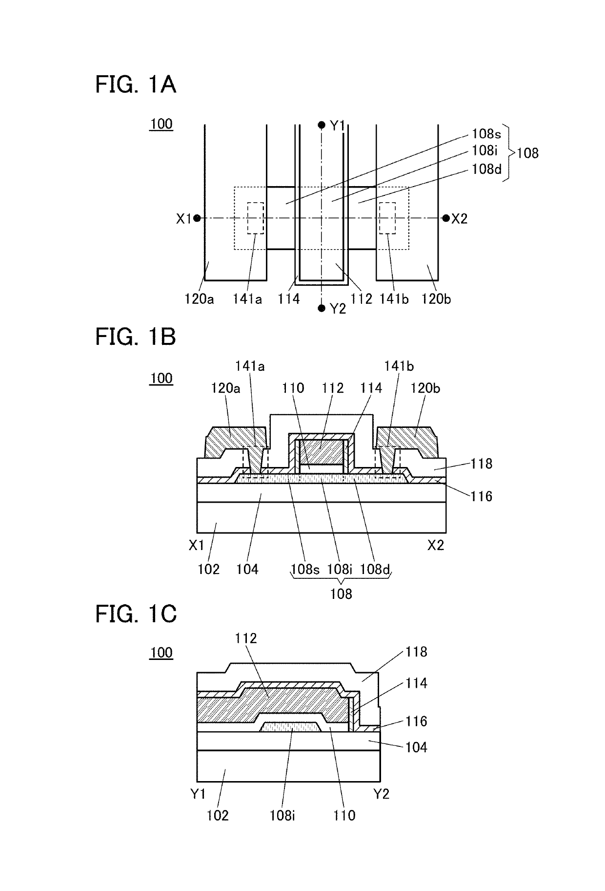
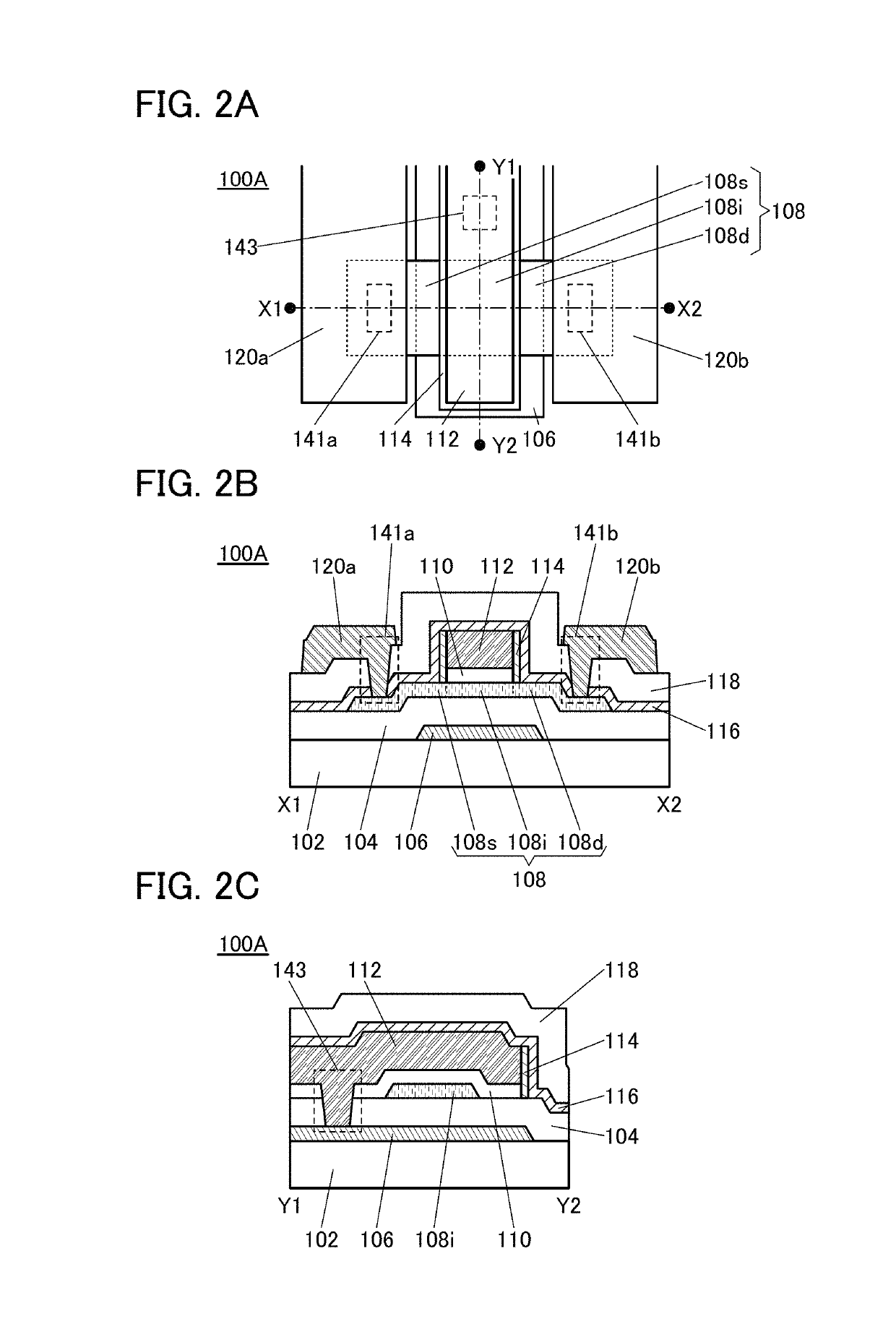
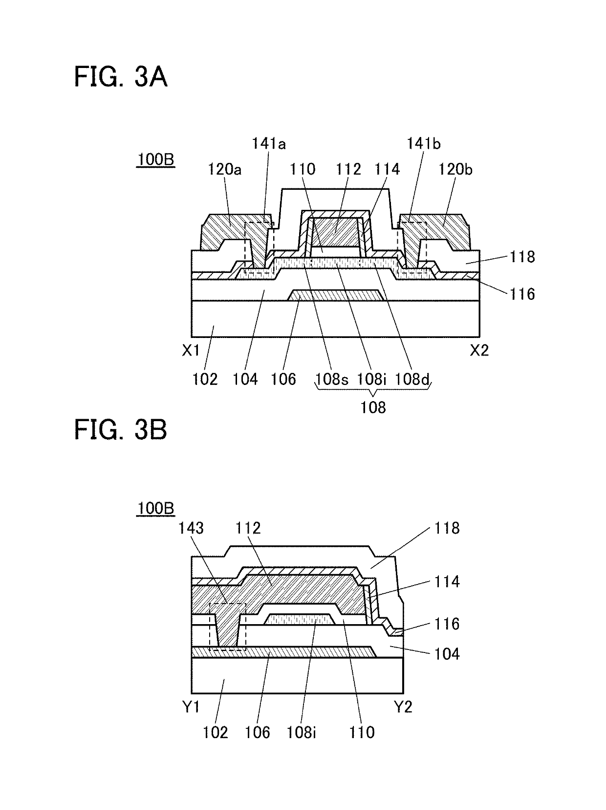
[0104]In this embodiment, examples of a semiconductor device including a transistor and a method for manufacturing the semiconductor device will be described with reference to FIGS. 1A to 1C through FIGS. 22A to 22C.

[0105]FIGS. 1A to 1C illustrate an example of a semiconductor device including a transistor. Note that the transistor in FIGS. 1A to 1C has a staggered (top-gate) structure.

[0106]FIG. 1A is a top view of a transistor 100. FIG. 1B is a cross-sectional view taken along dashed-dotted line X1-X2 in FIG. 1A. FIG. 1C is a cross-sectional view taken along dashed-dotted line Y1-Y2 in FIG. 1A. For clarity, FIG. 1A does not illustrate some components such as an insulating film 110. As in FIG. 1A, some components are not illustrated in some cases in top views of transistors described below. Furthermore, the direction of dashed-dotted line X1-X2 may be referred to as a channel length (L) direction, and the direction of dashed-dotted line Y1-Y2 may be referred to as a c...

embodiment 2

(Embodiment 2)

[0320]In this embodiment, the structure and the like of an oxide semiconductor will be described with reference to FIGS. 23A to 23E, FIGS. 24A to 24E, FIGS. 25A to 25D, FIGS. 26A and 26B, and FIG. 27.

[0321]An oxide semiconductor is classified into a single-crystal oxide semiconductor and a non-single-crystal oxide semiconductor. Examples of the non-single-crystal oxide semiconductor include a c-axis aligned crystalline oxide semiconductor (CAAC-OS), a polycrystalline oxide semiconductor, a nanocrystalline oxide semiconductor (nc-OS), an amorphous-like oxide semiconductor (a-like OS), and an amorphous oxide semiconductor.

[0322]From another perspective, an oxide semiconductor is classified into an amorphous oxide semiconductor and a crystalline oxide semiconductor. Examples of the crystalline oxide semiconductor include a single-crystal oxide semiconductor, a CAAC-OS, a polycrystalline oxide semiconductor, and an nc-OS.

[0323]An amorphous structure is generally thought to...

embodiment 3

(Embodiment 3)

[0362]In this embodiment, an example of a display device that includes the transistor described in the above embodiment will be described below with reference to FIG. 28, FIG. 29, and FIG. 30.

[0363]FIG. 28 is a top view illustrating an example of a display device. A display device 700 in FIG. 28 includes a pixel portion 702 provided over a first substrate 701, a source driver circuit portion 704 and a gate driver circuit portion 706 which are provided over the first substrate 701, a sealant 712 provided to surround the pixel portion 702, the source driver circuit portion 704, and the gate driver circuit portion 706, and a second substrate 705 provided to face the first substrate 701. The first substrate 701 and the second substrate 705 are sealed with the sealant 712. That is, the pixel portion 702, the source driver circuit portion 704, and the gate driver circuit portion 706 are enclosed by the first substrate 701, the sealant 712, and the second substrate 705. Altho...


PUM

PropertyMeasurementUnit
angleaaaaaaaaaa
angleaaaaaaaaaa
angleaaaaaaaaaa

Abstract

In a transistor including an oxide semiconductor, a change in electrical characteristics is suppressed and reliability is improved. The transistor includes an oxide semiconductor film over a first insulating film; a second insulating film over the oxide semiconductor film; a gate electrode over the second insulating film; a metal oxide film in contact with a side surface of the second insulating film; and a third insulating film over the oxide semiconductor film, the gate electrode, and the metal oxide film. The oxide semiconductor film includes a channel region overlapping with the gate electrode, a source region in contact with the third insulating film, and a drain region in contact with the third insulating film. The source region and the drain region contain one or more of hydrogen, boron, carbon, nitrogen, fluorine, phosphorus, sulfur, chlorine, titanium, and a rare gas.

Description

BACKGROUND OF THE INVENTION[0001]1. Field of the Invention[0002]One embodiment of the present invention relates to a semiconductor device including an oxide semiconductor film and a display device including the semiconductor device.[0003]Note that one embodiment of the present invention is not limited to the above technical field. The technical field of one embodiment of the invention disclosed in this specification and the like relates to an object, a method, or a manufacturing method. In addition, the present invention relates to a process, a machine, manufacture, or a composition of matter. In particular, one embodiment of the present invention relates to a semiconductor device, a display device, a light-emitting device, a power storage device, a memory device, a driving method thereof, or a manufacturing method thereof.[0004]In this specification and the like, a semiconductor device generally means a device that can function by utilizing semiconductor characteristics. A semicond...

Claims


Application Information

Patent Timeline
Patent Type & Authority Patents(United States)
IPC IPC(8): H01L29/786G06F3/041C23C14/08C23C14/34H01L27/12H01L29/04G06F3/044H01L29/66H01L29/24C23C16/455H01L27/146H01L27/105
CPCH01L29/78606C23C14/086C23C14/3414G06F3/044G06F3/0412H01L27/1052H01L27/1225H01L27/14616H01L29/045H01L29/24H01L29/66969H01L29/7869H01L29/78618H01L29/78696C23C14/08G06F2203/04103G06F2203/04102G06F1/1643G06F1/169H01L29/78633H01L29/78648H01L29/78693H01L27/1248G06F3/0443G06F3/0446H10B99/00
Inventor YAMAZAKI, SHUNPEIKOEZUKA, JUNICHIOKAZAKI, KENICHIJINTYOU, MASAMIIGUCHI, TAKAHIROGOTO, NAOTO
Owner SEMICON ENERGY LAB CO LTD
Why Eureka
Try Eureka