Compound for organic electronic element, organic electronic element using the same, and an electronic device thereof
a technology of electronic elements and organic electric elements, which is applied in the direction of luminescent compositions, isotope introduction to heterocyclic compounds, organic chemistry, etc., can solve the problems of power consumption, efficiency and life span, and the need to increase the need for power consumption, so as to improve luminescence efficiency, color purity and lifespan, the effect of improving the efficiency of luminescen
- Summary
- Abstract
- Description
- Claims
- Application Information
AI Technical Summary
Benefits of technology
Problems solved by technology
Method used
Image
Examples
synthesis example
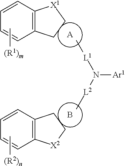
[0092]The compounds(final products) of the present invention represented by Formula 1 can be synthesized by reaction of Sub and Sub 2 as illustrated in, but not limited to, the following Reaction Scheme 1.
[0093]
[0094](X1, X2, A ring, B ring, Ar1, L1, L2, R1, R2, m and n are each the same as defined in Formula 1 above.)
[0095]I. Synthesis of Sub 1
[0096]Compound Sub 1 of Reaction Scheme 1 can be synthesized, but not limited to, by any one reaction of the following Reaction Schemes 2 to 4.
[0097]
[0098]
[0099]
[0100]In Reaction Schemes 2 to 4, R corresponds to (R1)m or (R2)n of Formula 1, X corresponds to X1 or X2 of Formula 1, L corresponds to L1 or L2 of Formula 1, and Z ring corresponds to A ring or B ring of Formula 1.
[0101]Synthesis Examples of compounds comprised in Sub 1 are as followings.
1. Synthesis Example of Sub 1-10
[0102]
[0103]2-(4-bromophenyl)-1-(methylsulfinyl)naphthalene (35.08 g, 101.6 mmol) as a starting material and triflic acid (134.9 ml, 1524.1 mmol) were loaded into a r...
example i-2
[Example I-2] to [Example I-65] Green Oled (a Hole Transport Layer)
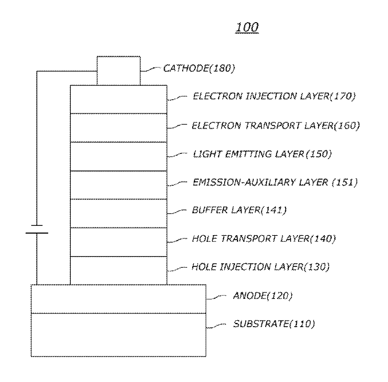
[0207]The OLEDs were manufactured in the same manner as described in Example I-1, except that any one of the compounds P-4 to P-200 of the present invention in the Table 4 below was used as the hole transport layer material of the light emitting layer, instead of the inventive compound P-1.
example ii-1
[Example II-1] Green OLED (an Emission-Auxiliary Layer)
[0224]Organic light emitting diodes (OLEDs) were fabricated according to a conventional method by using a compound of the present invention as an emission-auxiliary layer material.
[0225]First, an ITO layer (anode) was formed on a glass substrate, and then 2-TNATA was vacuum-deposited on the ITO layer to form a hole injection layer with a thickness of 60 nm.
[0226]Subsequently, N,N′-Bis(1-naphthalenyl)-N,N′-bis-phenyl-(1,1′-biphenyl)-4,4′-diamine (hereinafter, “NPB”) was vacuum-deposited with a thickness of 60 nm on the hole injection layer to form a hole transport layer.
[0227]Subsequently, the compound P-1 of the present invention was vacuum-deposited on the hole transport layer to form an emission-auxiliary layer with a thickness of 20 nm. A light emitting layer with a thickness of 30 nm was formed on the emission-auxiliary layer by using the CBP as a host material and Ir(ppy)3 as a dopant material in a weight ratio of 90:10.
[02...
PUM
| Property | Measurement | Unit |
|---|---|---|
| thickness | aaaaa | aaaaa |
| thickness | aaaaa | aaaaa |
| thickness | aaaaa | aaaaa |
Abstract
Description
Claims
Application Information


