Compound for organic electronic element, organic electronic element using the same, and an electronic device thereof

a technology of electronic elements and organic electric elements, applied in the direction of luminescent compositions, organic chemistry, chemistry apparatus and processes, etc., can solve the problems of power consumption, efficiency and life span issues, and the need for power consumption to increase, so as to achieve high luminescence efficiency, wide band gap, and high t1 energy value

Active Publication Date: 2019-02-14
DUK SAN NEOLUX
View PDF6 Cites 0 Cited by
  • Summary
  • Abstract
  • Description
  • Claims
  • Application Information

AI Technical Summary

Benefits of technology

[0014]In order to solve one or more of the above-mentioned problems occurring in the prior art, an aspect of the present invention is to provide a compound which allows an organic electric element to improve in luminescence efficiency, stability and lifespan, an organic electric element containing the same, and an electronic device including the organic electric element.
[0017]By employing the compound of the present invention that has wide band gap and high T1 energy value due to the non-linear linker (L) attached to the carbazole core, the organic electric element according to one or more embodiments of the present invention can have not only high luminescence efficiency and high heat-resistance, but also significantly improved color purity and lifespan.

Problems solved by technology

Currently, the power consumption is required more and more as size of display becomes larger and larger in the portable display market.
Therefore, the power consumption is a very important factor in the portable display with a limited power source of the battery, and efficiency and life span issue also must be solved.
However, efficiency cannot be maximized only by simply improving the organic material layer.
Due to this, excitons generated from a light emitting layer are transported to the hole transporting layer, resulting in a charge unbalance in the light emitting layer.
Thus, light emission occurs in the hole transporting layer or at an interface of the hole transporting layer so that the organic electroluminescent device is reduced in color purity, efficiency, and lifespan.
Also, when using a material having rapid hole mobility for reducing a driving voltage, this is tend to decrease the efficiency.
In an OLEDs, a charge unbalance in the light emitting layer is caused because of that hole mobility is faster than electron mobility, and reduced efficiency and lifespan is happened.
However, such a stable and efficient organic material layer material for an organic electric element has not yet been fully developed.

Method used


Image

  • Compound for organic electronic element, organic electronic element using the same, and an electronic device thereof
  • Compound for organic electronic element, organic electronic element using the same, and an electronic device thereof
  • Compound for organic electronic element, organic electronic element using the same, and an electronic device thereof

Examples


synthesis example

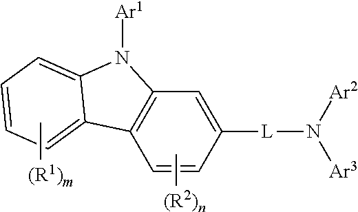
[0099]The final product of the present invention can be synthesized by reaction of Sub 1 and Sub 2 as illustrated in the following Reaction Scheme 1, but the present invention is not limited to the following examples.

I. Synthesis Example of Sub 1

[0100]Sub 1 of the Reaction Scheme 1 can be synthesized according to, but not limited to, the following Reaction Scheme 2.

1. Synthesis Example of Sub 1-1

(1) Synthesis of Sub 1-I-1

[0101]

[0102]Phenylboronic acid (76.84 g, 630.2 mmol) was dissolved in THF (2780 ml) in a round bottom flask. Then, 4-bromo-1-iodo-2-nitrobenzene (309.96 g, 945.3 mmol), Pd(PPh3)4 (36.41 g, 31.5 mmol), K2CO3 (261.3 g, 1890.6 mmol) and water (1390 ml) were added into the round bottom flask, and the mixture was stirred at 80° C. After the completion of the reaction, the reaction product was extracted with CH2Cl2 and water. The extracted organic layer was dried over MgSO4 and concentrated. The concentrated resultant was separated by silica gel column chromatography, and...

example 1

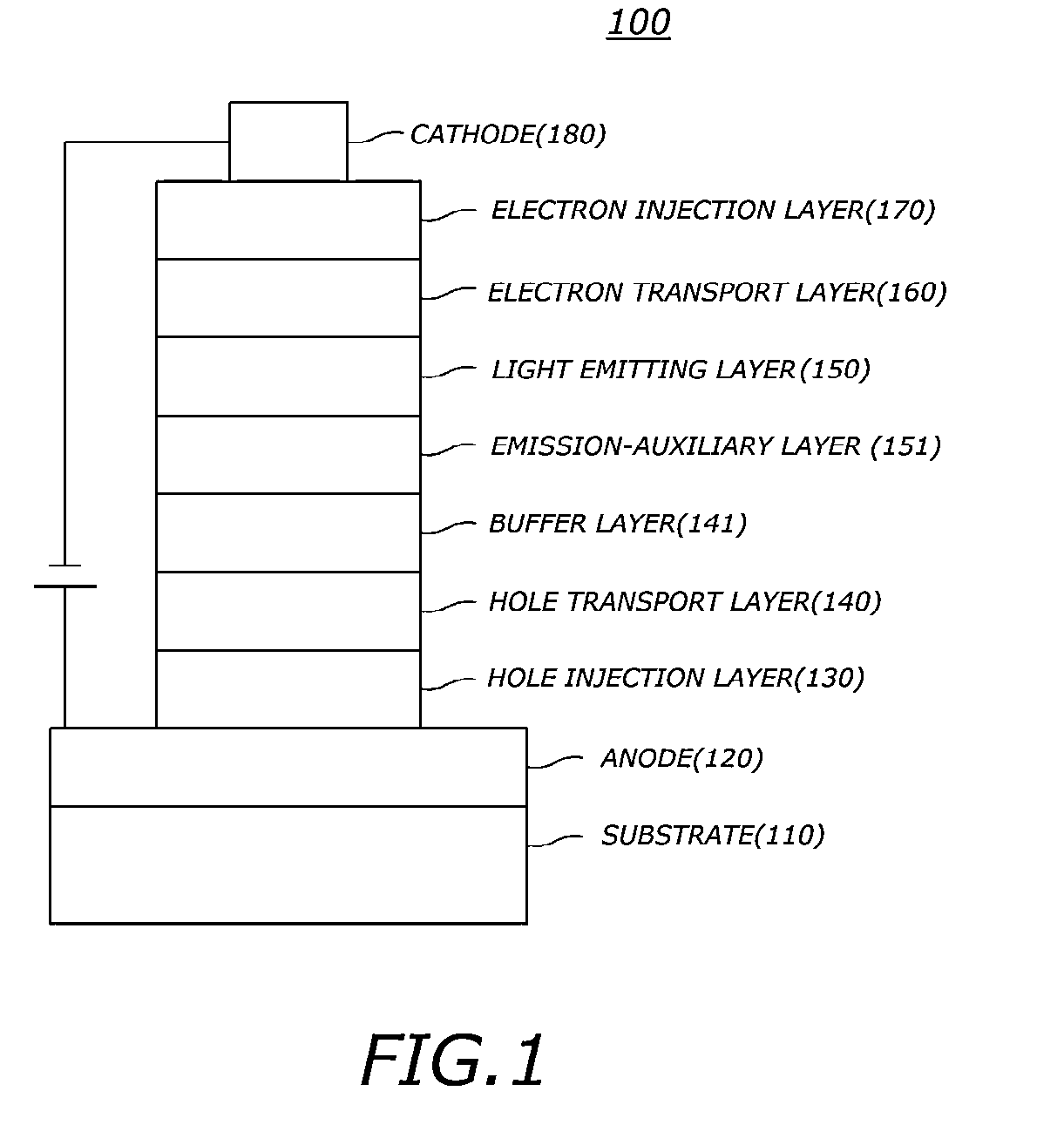
[Example 1] Green OLEDs (A Hole Transport Layer)

[0247]Organic light emitting diodes (OLEDs) were fabricated according to a conventional method by using a compound of the present invention as a hole transport layer material.

[0248]First, an ITO layer (anode) was formed on a glass substrate, and a film of 4,4′,4″-Tris[2-naphthyl(phenyl)amino]triphenylamine (“2-TNATA”) was vacuum-deposited on the ITO layer to form a hole injection layer with a thickness of 60 nm. Subsequently, P1-1 of the present invention was vacuum-deposited with a thickness of 60 nm on the hole injection layer to form a hole transport layer.

[0249]Subsequently, a light emitting layer with a thickness of 30 nm was deposited on the hole transport layer by doping the hole transport layer with 4,4′-N,N′-dicarbazole-biphenyl (“CBP”) as a host material and tris(2-phenylpyridine)-iridium (“Ir(ppy)3)”) as a dopant material in a weight ratio of 90:10.

[0250]Next, a film of ((1,1′-bisphenyl)-4-olato)bis(2-methyl-8-quinolinolato)...

example 256

[Example 2] to [Example 256] Green OLEDs (A Hole Transport Layer)

[0252]The OLEDs were manufactured in the same manner as described in Example 1, except that any one of the compounds P1-2 to P1-112, P2-1 to P2-112, P3-1 to P3-6, P3-19 to P3-24, P3-37 and P3-38 of the present invention in the Table 4 below was used as the hole transport layer material, instead of the inventive compound P1-1.


PUM

PropertyMeasurementUnit
thicknessaaaaaaaaaa
thicknessaaaaaaaaaa
thicknessaaaaaaaaaa

Abstract

Provided are a compound of Formula 1 and an organic electric element including a first electrode, a second electrode, and an organic material layer between the first electrode and the second electrode and comprising the compound, the element showing improved luminescence efficiency, stability, and life span.

Description

CROSS-REFERENCE TO RELATED APPLICATION[0001]This patent application claims benefit under 35 U.S.C. 119(e), 120, 121, or 365(c), and is a National Stage entry from International Application No. PCT / KR2015 / 001801 filed on Feb. 25, 2015, which claims priority to Korean Patent Application No. 10-2014-0023356 filed on Feb. 27, 2014, Korean Patent Application No. 10-2014-0064727 filed on May 28, 2014, and Korean Patent Application No. 10-2015-0025588 filed on Feb. 24, 2015, the contents of which are hereby incorporated by reference for all purposes as if fully set forth herein.BACKGROUNDTechnical Field[0002]The present invention relates to compounds for organic electric elements, organic electric elements using the same, and electronic devices thereof.Background Art[0003]In general, an organic light emitting phenomenon refers to a phenomenon in which electric energy is converted into light energy of an organic material. An organic electric element utilizing the organic light emitting phen...

Claims


Application Information

Patent Timeline
Patent Type & Authority Applications(United States)
IPC IPC(8): H01L51/00C09K11/06C07D209/86C07D409/12C07D409/04
CPCH01L51/0061C09K11/06C07D209/86H01L51/006C07D409/12H01L51/5088C09K2211/185H01L51/0072H01L51/0052H01L51/0074C07D409/04C09K2211/1007C09K2211/1014C09K2211/1029C09K2211/1044C09K2211/1088C09K2211/1092H10K85/636H10K85/633H10K85/631H10K85/615H10K85/324H10K85/654H10K85/6576H10K85/6574H10K85/342H10K85/6572H10K50/15C07D403/14Y02E10/549H10K50/18H10K50/156H10K50/11H10K50/17
Inventor MUN, SOUNG YUNLEE, SUN-HEEPARK, JUNG CHEOLKIM, DAESUNGLEE, BUM SUNGPARK, SEONG JE
Owner DUK SAN NEOLUX
Why Eureka
Try Eureka